
アプリケーション・ノート (1)
データ・シート (1)
パッケージ情報 (3)
-
Standard product orientation 12NC ending 115[SOT1161-1_115]
ユーザ・ガイド (2)
-
PCA9632 demonstration board OM13269[UM10528]
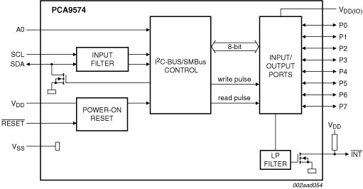
The PCA9574 is a CMOS device that provides 8 bits of General Purpose parallel Input/Output (GPIO) expansion in low voltage processor and handheld battery powered mobile applications and was developed to enhance the NXP family of I²C-bus I/O expanders. The improvements include lower supply current, lower operating voltage of 1.1 V to 3.6 V, dual and separate supply rails to allow voltage level translation anywhere between 1.1 V and 3.6 V, 400 kHz clock frequency, and smaller packaging. Any of the eight I/O ports can be configured as an input or output independent of each other and default on start-up to inputs. I/O expanders provide a simple solution when additional I/Os are needed while keeping interconnections to a minimum; for example in battery powered mobile applications and clamshell devices for interfacing to sensors, push buttons, keypad, etc. In addition to providing a flexible set of GPIOs, it simplifies interconnection of a processor running at one voltage level to I/O devices operating at a different (usually higher) voltage level. PCA9574 has built-in level shifting feature that makes these devices extremely flexible in mixed signal environments where communication between incompatible I/Os is required. The core of PCA9574 can operate at a voltage as low as 1.1 V while the I/O bank can operate in the range 1.1 V to 3.6 V. Bus-hold with programmable on-chip pull-up or pull-down feature for I/Os is also provided.
The system controller can enable the I/Os as either inputs or outputs by writing to the I/O configuration register bits. The data for each input or output is kept in the corresponding Input or Output register. The polarity of the read register can be inverted with the Polarity inversion register (active HIGH or active LOW operation). Either a bus-hold function or pull-up/pull-down feature can be selected by programming corresponding registers. The bus-hold provides a valid logic level when the I/O bus is not actively driven. When bus-hold feature is not selected, the I/O ports can be configured to have pull-up or pull-down by programming the pull-up/pull-down configuration register.
An open-drain interrupt output pin (INT) allows monitoring of the input pins and is asserted each time a change occurs on an input port unless that port is masked (default = masked). A ‘GPIO All Call’ command allows programming multiple PCA9574s at the same time even if they have different individual I²C-bus addresses. This allows optimal code programming when more than one device needs to be programmed with the same instruction or if all outputs need to be turned on or off at the same time. The internal Power-On Reset (POR) or hardware reset pin (RESET) initializes the eight I/Os as inputs, sets the registers to their default values and initializes the device state machine. The I/O bank is held in its default state when the logic supply (VDD) is off.
One address select pin allows up to two PCA9574 devices to be connected with two different addresses on the same I²C-bus.
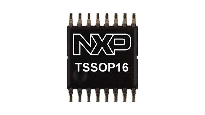
The PCA9574 is available in TSSOP16 and HVQFN16 packages and is specified over the -40 °C to +85 °C industrial temperature range.
図を選択する。:
|
|
|
|
|
|
|
|---|---|---|---|---|---|
|
|
|
|
|
|
|
|
|
|
|
|
|
|
|
|
|
|
|
|
|
|
|
|
|
|
|
|
|
|
|
|
|
|
|
|
|
|
|
|
|
|
|
|
|
|
|
|
|
|
|
|
|
|
|
|
|
|
|
|
|
|
|
|
|
|
|
|
|
|
クイック・リファレンス ドキュメンテーションの種類
10 ドキュメント
コンパクトリスト
3 設計・ファイル
完全な内訳を受け取ります。 製品の設置面積などについては、 eCad ファイル.
NXPから直接サポートを受けるには、以下のサイトをご覧ください。 エンジニアリング・サービス.
1 エンジニアリング・サービス

この製品をサポートするその他のパートナー製品を見つけるには、当社の Web サイトにアクセスしてください パートナーマーケットプレイス.