
アプリケーション・ノート (3)
カタログ (1)
サポート情報 (1)
-
Footprint for wave soldering[SSOP-TSSOP-VSO-WAVE]
データ・シート (1)
パッケージ情報 (2)
ユーザ・ガイド (2)
-
PCA9698 demonstration board OM6281[UM10267]
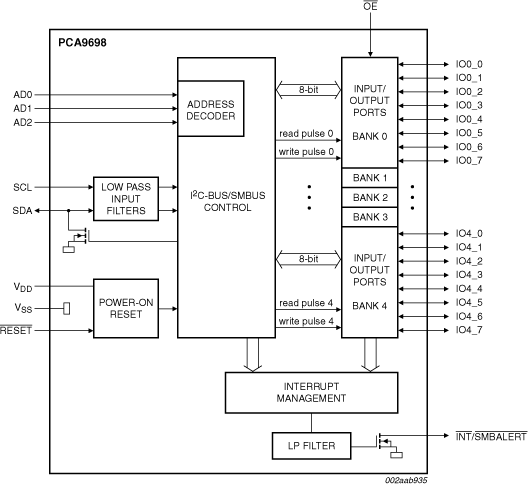
The PCA9698 provides 40-bit parallel input/output (I/O) port expansion for I²C-bus applications organized in 5 banks of 8 I/Os. At 5 V supply voltage, the outputs are capable of sourcing 10 mA and sinking 25 mA with a total package load of 1 A to allow direct driving of 40 LEDs. Any of the 40 I/O ports can be configured as an input or output.
The PCA9698 is the first GPIO device in a new Fast-mode Plus (Fm+) family. Fm+ devices offer higher frequency (up to 1 MHz) and longer, more densely populated bus operation (up to 4000 pF).
The device is fully configurable: output ports can be programmed to be totem-pole or open-drain and logic states can change at either the Acknowledge (bank change) or the Stop Command (global change), each input port can be masked to prevent it from generating interrupts when its state changes, I/O data logic state can be inverted when read by the system controller.
An open-drain interrupt output pin (INT) allows monitoring of the input pins and is asserted each time a change occurs in one or several input ports (unless masked).
The Output Enable pin (OE) 3-states any I/O selected as output and can be used as an input signal to blink or dim LEDs (PWM with frequency > 80 Hz and change duty cycle).
A 'GPIO All Call' command allows to program multiple Advanced GPIOs at the same time even if they have different I²C-bus addresses. This allows optimal code programming when more than one device needs to be programmed with the same instruction or if all outputs need to be turned on or off at the same time (for example, LED test).
The Device ID, hard coded in the PCA9698, allows the system controller to read manufacturer, part type and revision information.
The SMBus Alert feature allows the SMBALERT pins of multiple devices with this feature to be connected together to form a wired-AND signal and to be used in conjunction with the SMBus Alert Response Address.
The internal Power-On Reset (POR) or hardware reset pin (RESET) initializes the 40 I/Os as inputs. Three address select pins configure one of 64 target addresses.
The PCA9698 is available in 56-pin TSSOP and HVQFN packages and is specified over the -40 °C to +85 °C industrial temperature range.
|
|
|
|
|
|
|
|---|---|---|---|---|---|
|
|
|
|
|
|
|
|
|
|
|
|
|
|
|
|
|
|
|
|
|
|
|
|
|
|
|
|
|
|
|
|
|
|
|
|
|
|
|
|
|
|
|
|
|
|
|
|
|
|
|
|
|
|
|
|
|
|
|
|
|
|
|
|
|
|
|
|
|
|
クイック・リファレンス ドキュメンテーションの種類
1-10 件/全 12 ドキュメント
コンパクトリスト
NXPから直接サポートを受けるには、以下のサイトをご覧ください。 エンジニアリング・サービス.
1 エンジニアリング・サービス

この製品をサポートするその他のパートナー製品を見つけるには、当社の Web サイトにアクセスしてください パートナーマーケットプレイス.