
アプリケーション・ノート (2)
カタログ (2)
データ・シート (1)
パッケージ情報 (1)
ユーザ・ガイド (3)
-
PCA9632 demonstration board OM13269[UM10528]
-
PCA9698 demonstration board OM6281[UM10267]
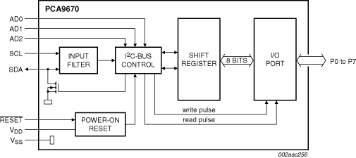
The PCA9670 provides general-purpose remote I/O expansion via the two-wire bidirectional I²C‑bus (serial clock (SCL), serial data (SDA)).
The devices consist of eight quasi-bidirectional ports, 1 MHz 30 mA drive I²C‑bus interface, three hardware address inputs and a reset input operating between 2.3 V and 5.5 V. 1 MHz I²C‑bus Fast‑mode Plus (Fm+) can support PWM dimming of LEDs, and higher I²C‑bus drive 30 mA allows more devices to be on the bus without the need for bus buffers. The quasi-bidirectional port can be independently assigned as an input to monitor interrupt status or keypads, or as an output to activate indicator devices such as LEDs. The system controller can read from the input port or write to the output port through a single register
The low current consumption of 2.5 μA (typical, static) is great for mobile applications and the latched output ports have 25 mA high current sink drive capability for directly driving LEDs.
The PCA9670 has three hardware address pins and allows up to 64 of these PCA9670 I/O expanders on the same I²C‑bus without the need for bus buffers, supporting up to 512 I/Os (for example, 512 LEDs).
The internal Power-On Reset (POR) and active LOW hardware reset pin (RESET) initialize the I/Os as inputs with a weak internal pull-up 100 μA current source.
|
|
|
|
|
|
|
|---|---|---|---|---|---|
|
|
|
|
|
|
|
|
|
|
|
|
|
|
|
|
|
|
|
|
|
|
|
|
|
|
|
|
|
|
|
|
|
|
|
|
|
|
|
|
|
|
|
|
|
|
|
|
|
|
|
|
|
|
|
|
|
|
|
|
|
|
|
|
|
|
|
|
|
|
クイック・リファレンス ドキュメンテーションの種類
10 ドキュメント
コンパクトリスト
2 設計・ファイル
完全な内訳を受け取ります。 製品の設置面積などについては、 eCad ファイル.
NXPから直接サポートを受けるには、以下のサイトをご覧ください。 エンジニアリング・サービス.
1 エンジニアリング・サービス

この製品をサポートするその他のパートナー製品を見つけるには、当社の Web サイトにアクセスしてください パートナーマーケットプレイス.
