アプリケーション・ノート (2)
カタログ (1)
データ・シート (1)
-
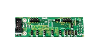
16-bit I2C-Bus and SMBus, low power I/O port with interrupt[PCA9535_PCA9535C]
パッケージ情報 (4)
ユーザ・ガイド (2)
-
PCA9632 demonstration board OM13269[UM10528]
The PCA9535 and PCA9535C are 24-pin CMOS devices that provide 16 bits of General Purpose parallel Input/Output (GPIO) expansion for I²C-bus/SMBus applications and was developed to enhance the NXP Semiconductors family of I²C-bus I/O expanders. The improvements include higher drive capability, 5 V I/O tolerance, lower supply current, individual I/O configuration and smaller packaging. I/O expanders provide a simple solution when additional I/O is needed for ACPI power switches, sensors, push buttons, LEDs, fans, etc.
The PCA9535 and PCA9535C consist of two 8-bit Configuration (Input or Output selection), Input, Output and Polarity Inversion (active HIGH or active LOW operation) registers. The system controller can enable the I/Os as either inputs or outputs by writing to the I/O configuration bits. The data for each input or output is kept in the corresponding Input or Output register. The polarity of the read register can be inverted with the Polarity Inversion register. All registers can be read by the system controller. Although pin-to-pin and I²C-bus address compatible with the PCF8575, software changes are required due to the enhancements and are discussed in Application Note AN469.
The PCA9535 is identical to the PCA9555 except for the removal of the internal I/O pull-up resistor which greatly reduces power consumption when the I/Os are held LOW.
The PCA9535C is identical to the PCA9535 except that all the I/O pins are high-impedance open-drain outputs.
The PCA9535 and PCA9535C open-drain interrupt output is activated when any input state differs from its corresponding Input Port register state and is used to indicate to the system controller that an input state has changed. The power-on reset sets the registers to their default values and initializes the device state machine.
Three hardware pins (A0, A1, A2) vary the fixed I²C-bus address and allow up to eight devices to share the same I²C-bus/SMBus. The fixed I²C-bus address of the PCA9535 and PCA9535C are the same as the PCA9555 allowing up to eight of these devices in any combination to share the same I²C-bus/SMBus.
|
|
|
|
|
|
|
|---|---|---|---|---|---|
|
|
|
|
|
|
|
|
|
|
|
|
|
|
|
|
|
|
|
|
|
|
|
|
|
|
|
|
|
|
|
|
|
|
|
|
|
|
|
|
|
|
|
|
|
|
|
|
|
|
|
|
|
|
|
|
|
|
|
|
|
|
|
|
|
|
|
|
|
|
クイック・リファレンス ドキュメンテーションの種類
1-10 件/全 14 ドキュメント
コンパクトリスト
1-5件/全 8 設計・ファイル
完全な内訳を受け取ります。 製品の設置面積などについては、 eCad ファイル.
NXPから直接サポートを受けるには、以下のサイトをご覧ください。 エンジニアリング・サービス.
1 エンジニアリング・サービス

この製品をサポートするその他のパートナー製品を見つけるには、当社の Web サイトにアクセスしてください パートナーマーケットプレイス.