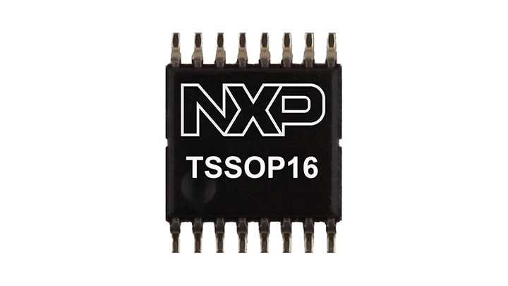
The PCA9500 is an 8-bit I/O expander with an on-board 2-kbit EEPROM.
The I/O expander's eight quasi-bidirectional data pins can be independently assigned as inputs or outputs to monitor board level status or activate indicator devices such as LEDs. The system writes to the I/O configuration bits in the same way as for the PCF8574. The data for each input or output is kept in the corresponding Input or Output register. The system leader can read all registers.
The EEPROM can be used to store error codes or board manufacturing data for read-back by application software for diagnostic purposes and is included in the I/O expander package.
The PCA9500 has 3 address pins with internal pull-up resistors allowing up to 8 devices to share the common two-wire I²C software protocol serial data bus. The fixed GPIO I²C-bus address is the same as the PCF8574 and the fixed EEPROM I²C-bus address is the same as the PCF8582C-2, so the PCA9500 appears as two separate devices to the bus leader.
The PCA9500 supports hot insertion to facilitate usage in removable cards on backplane systems.
The PCA9501 is an alternative to the functionally similar PCA9500 for systems where a higher number of devices are required to share the same I²C-bus or an interrupt output is required.


