

MCX N94、N54、N53、N52、N24:高集積の低消費電力デュアル・コアArm® Cortex®-M33 MCUにオンチップ・アクセラレータおよび高度なセキュリティを搭載
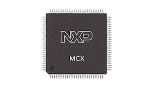
MCX A17ファミリは、モータ制御アプリケーション向けに最適化されており、優れた性能と高度な統合を実現します。最大180 MHzで動作するArm® Cortex®-M33コアを搭載しています。MCX A17ファミリが搭載する2つのFlexPWMはそれぞれ4つのサブモジュールを備え、各サブモジュールのAOIロジックによって、高度なモータ制御が可能になります。また、最大2つのADC、効率的なデータ処理のためのSmartDMAに加え、I3C、CAN FD、USB、FlexIOなどの豊富なシリアル・インターフェースも備えています。
MCX A175およびA176は、最大1 MBのフラッシュと256 KBのRAMを搭載しています。MCX A173およびA174は、最大256 KBのフラッシュと64 KBのRAMを搭載しています。こうした特長が、アプリケーションのニーズに合わせた柔軟な開発を可能にします。MCX A17デバイスはMCUXpresso開発者エクスペリエンスでサポートされており、その包括的なツール群によって、開発を簡素化し、市場投入までの時間を短縮できます。
図を選択する。:
| 製品 | メイン・クロック | フラッシュ | 特長 | パッケージ | FRDMボード |
|---|---|---|---|---|---|
| MCXA173 | 180 MHz | 128 KB | ADC x 2、オペアンプ x 1、USB、CAN x 1 | H-PQFN32 LQFP48 LQFP64 LQFP100 | FRDM-MCXA174 |
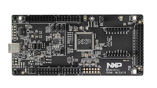
| MCXA174 | 180 MHz | 256 KB | ADC x 2、オペアンプ x 1、USB、CAN x 1 | H-PQFN32 LQFP48 LQFP64 LQFP100 | FRDM-MCXA174 |
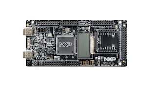
| MCXA175 | 180 MHz | 512 KB | ADC x 2、オペアンプ x 1、USB、CAN x 1 | LQFP64 LQFP100 LQFP144 WFBGA169 | FRDM-MCXA266 |
| MCXA176 | 180 MHz | 1024 KB | ADC x 2、オペアンプ x 1、USB、CAN x 1 | LQFP64 LQFP100 LQFP144 WFBGA169 | FRDM-MCXA266 |
MCX N94、N54、N53、N52、N24:高集積の低消費電力デュアル・コアArm® Cortex®-M33 MCUにオンチップ・アクセラレータおよび高度なセキュリティを搭載
MCX A14x/15x MCU:Arm® Cortex® M33、拡張性の高いデバイス・オプション、低消費電力でインテリジェントなペリフェラルを搭載
High Efficiency Arm® Cortex®-M33-Based Microcontroller Family
LPC552x/S2x: Mainstream Arm® Cortex®-M33-based Microcontroller Family
|
|
|
|
|
|
|
|---|---|---|---|---|---|
|
|
|
|
|
|
|
|
|
|
|
|
|
|
|
|
|
|
|
|
|
|
|
|
|
|
|
|
|
|
|
|
|
|
|
|
|
|
|
|
|
|
|
|
|
|
|
|
|
|
|
|
|
|
|
|
|
|
|
|
|
|
|
|
|
|
|
|
|
|
クイック・リファレンス ドキュメンテーションの種類
1-10 件/全 15 ドキュメント
コンパクトリスト
4 設計・ファイル
完全な内訳を受け取ります。 製品の設置面積などについては、 eCad ファイル.
4 ハードウェア提供
クイック・リファレンス ソフトウェア・タイプ.
5 ソフトウェア・ファイル
追加ソフトウェアを利用可能 パートナー・ソリューションの特集を表示.
注: より快適にご利用いただくために、ソフトウェアのダウンロードはデスクトップで行うことを推奨します。