Single-chip 16-bit/32-bit micro; 512 kB flash, Ethernet, CAN, LCD, USB 2.0 device/host/OTG, external memory interface

  • このページでは、新規設計を推奨しない製品に関する情報を掲載しています。

製品画像を見る

製品詳細

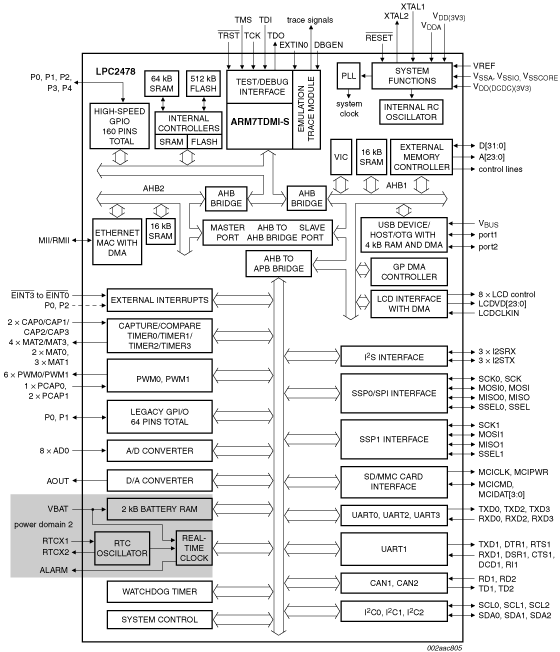
ブロック図

Block diagram: LPC2478FBD208, LPC2478FET208

Features

  • Arm7TDMI-S processor, running at up to 72 MHz.
  • 512 kB on-chip flash program memory with In-System Programming (ISP) and In-Application Programming (IAP) capabilities. Flash program memory is on the Arm local bus for high performance CPU access.
  • 98 kB on-chip SRAM includes:
    • 64 kB of SRAM on the Arm local bus for high performance CPU access.
    • 16 kB SRAM for Ethernet interface. Can also be used as general purpose SRAM.
    • 16 kB SRAM for general purpose DMA use also accessible by the USB.
    • 2 kB SRAM data storage powered from the Real-Time Clock (RTC) power domain.
  • LCD controller, supporting both Super-Twisted Nematic (STN) and Thin-Film Transistors (TFT) displays.
    • Dedicated DMA controller.
    • Selectable display resolution (up to 1024 × 768 pixels).
    • Supports up to 24-bit true-color mode.
  • Dual Advanced High-performance Bus (AHB) system allows simultaneous Ethernet DMA, USB DMA, and program execution from on-chip flash with no contention.
  • EMC provides support for asynchronous static memory devices such as RAM, ROM and flash, as well as dynamic memories such as single data rate SDRAM.
  • Advanced Vectored Interrupt Controller (VIC), supporting up to 32 vectored interrupts.
  • General Purpose DMA (GPDMA) controller on AHB that can be used with the SSP, I²S-bus, and SD/MMC interface as well as for memory-to-memory transfers.
  • Serial Interfaces:
    • Ethernet MAC with MII/RMII interface and associated DMA controller. These functions reside on an independent AHB.
    • USB 2.0 full-speed dual port device/host/OTG controller with on-chip PHY and associated DMA controller.
    • Four UARTs with fractional baud rate generation, one with modem control I/O, one with IrDA support, all with FIFO.
    • CAN controller with two channels.
    • SPI controller.
    • Two SSP controllers, with FIFO and multi-protocol capabilities. One is an alternate for the SPI port, sharing its interrupt. SSPs can be used with the GPDMA controller.
    • Three I²C-bus interfaces (one with open-drain and two with standard port pins).
    • I²S (Inter-IC Sound) interface for digital audio input or output. It can be used with the GPDMA.
  • Other peripherals:
    • SD/MMC memory card interface.
    • 160 General purpose I/O pins with configurable pull-up/down resistors.
    • 10-bit ADC with input multiplexing among 8 pins.
    • 10-bit DAC.
    • Four general purpose timers/counters with 8 capture inputs and 10 compare outputs. Each timer block has an external count input.
    • Two PWM/timer blocks with support for three-phase motor control. Each PWM has an external count input.
    • RTC with separate power domain. Clock source can be the RTC oscillator or the APB clock.
    • 2 kB SRAM powered from the RTC power pin, allowing data to be stored when the rest of the chip is powered off.
    • WatchDog Timer (WDT). The WDT can be clocked from the internal RC oscillator, the RTC oscillator, or the APB clock.
  • Single 3.3 V power supply (3.0 V to 3.6 V).
  • 4 MHz internal RC oscillator trimmed to 1 % accuracy that can optionally be used as the system clock.
  • Four reduced power modes: idle, sleep, power-down and deep power-down.
  • Four external interrupt inputs configurable as edge/level sensitive. All pins on port 0 and port 2 can be used as edge sensitive interrupt sources.
  • Processor wake-up from Power-down mode via any interrupt able to operate during Power-down mode (includes external interrupts, RTC interrupt, USB activity, Ethernet wake-up interrupt, CAN bus activity, port 0/2 pin interrupt).
  • Two independent power domains allow fine tuning of power consumption based on needed features.
  • Each peripheral has its own clock divider for further power saving. These dividers help reduce active power by 20 % to 30 %.
  • Brownout detect with separate thresholds for interrupt and forced reset.
  • On-chip power-on reset.
  • On-chip crystal oscillator with an operating range of 1 MHz to 25 MHz.
  • On-chip PLL allows CPU operation up to the maximum CPU rate without the need for a high frequency crystal. May be run from the main oscillator, the internal RC oscillator, or the RTC oscillator.
  • Boundary scan for simplified board testing.
  • Versatile pin function selections allow more possibilities for using on-chip peripheral functions.
  • Standard Arm test/debug interface for compatibility with existing tools.
  • Emulation trace module supports real-time trace.

Target Applications

  • Industrial control
  • Medical systems
  • Portable electronics
  • Point-of-Sale (POS) equipment

部品番号: LPC2478FET208.

購入/パラメータ


ドキュメント

クイック・リファレンス ドキュメンテーションの種類.

1-5 の 18 ドキュメント

全て表示

デザイン・ファイル

クイック・リファレンス 設計・ファイルの種類.

2 設計・ファイル

ソフトウェア

クイック・リファレンス ソフトウェア・タイプ.

2 ソフトウェア・ファイル

注: より快適にご利用いただくために、ソフトウェアのダウンロードはデスクトップで行うことを推奨します。

サポート

お困りのことは何ですか??