Single-chip 16/32-bit microcontrollers; 32/64/128/256/512 kB ISP/IAP flash with 10-bit ADC and DAC

  • このページでは、新規設計を推奨しない製品に関する情報を掲載しています。

製品画像を見る

製品詳細

ブロック図

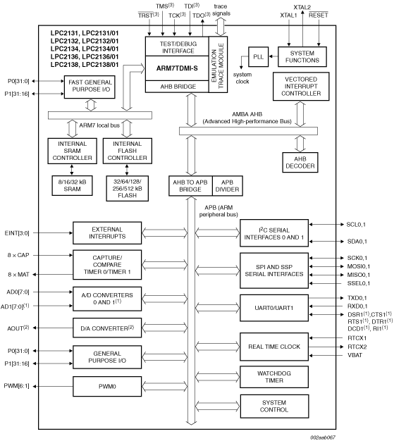
Block diagram: LPC2131FBD64, LPC2132FBD64, LPC2132FHN64, LPC2134FBD64, LPC2136FBD64, LPC2138FBD64, LPC2138FHN64

Features

2.1 Enhancements brought by LPC213x/01 devices
  • Fast GPIO ports enable port pin toggling up to 3.5 times faster than the original LPC213x. They also allow for a port pin to be read at any time regardless of its function.
  • Dedicated result registers for ADC(s) reduce interrupt overhead.
  • UART0/1 include fractional baud rate generator, auto-bauding capabilities and handshake flow-control fully implemented in hardware.
  • Additional BOD control enables further reduction of power consumption.

2.2 Key features common for LPC213x and LPC213x/01

  • 16/32-bit Arm7TDMI-S microcontroller in a tiny LQFP64 or HVQFN64 package.
  • 8/16/32 kB of on-chip static RAM and 32/64/128/256/512 kB of on-chip flash program memory. 128-bit wide interface/accelerator enables high-speed 60 MHz operation.
  • In-System Programming/In-Application Programming (ISP/IAP) via on-chip bootloader software. Single flash sector or full chip erase in 400 ms and programming of 256 B in 1 ms.
  • EmbeddedICE RT and Embedded Trace interfaces offer real-time debugging with the on-chip RealMonitor software and high-speed tracing of instruction execution.
  • One (LPC2131/32) or two (LPC2134/36/38) 8-channel 10-bit ADCs provide a total of up to 16 analog inputs, with conversion times as low as 2.44 µs per channel.
  • Single 10-bit DAC provides variable analog output (LPC2132/34/36/38).
  • Two 32-bit timers/external event counters (with four capture and four compare channels each), PWM unit (six outputs) and watchdog.
  • Low power Real-time clock with independent power and dedicated 32 kHz clock input.
  • Multiple serial interfaces including two UARTs (16C550), two Fast I²C-bus (400 kbit/s), SPI and SSP with buffering and variable data length capabilities.
  • Vectored interrupt controller with configurable priorities and vector addresses.
  • Up to forty-seven 5 V tolerant general purpose I/O pins in tiny LQFP64 or HVQFN package.
  • Up to nine edge or level sensitive external interrupt pins available.
  • 60 MHz maximum CPU clock available from programmable on-chip PLL with settling time of 100 µs.
  • On-chip integrated oscillator operates with external crystal in range of 1 MHz to 30 MHz and with external oscillator up to 50 MHz.
  • Power saving modes include Idle and Power-down.
  • Individual enable/disable of peripheral functions as well as peripheral clock scaling down for additional power optimization.
  • Processor wake-up from Power-down mode via external interrupt or BOD.
  • Single power supply chip with POR and BOD circuits:
    • CPU operating voltage range of 3.0 V to 3.6 V (3.3 V ± 10 %) with 5 V tolerant I/O pads.

部品番号: LPC2136FBD64.

購入/パラメータ


ドキュメント

クイック・リファレンス ドキュメンテーションの種類.

1-5 の 28 ドキュメント

全て表示

デザイン・ファイル

クイック・リファレンス 設計・ファイルの種類.

3 設計・ファイル

ソフトウェア

クイック・リファレンス ソフトウェア・タイプ.

1 ソフトウェア・ファイル

注: より快適にご利用いただくために、ソフトウェアのダウンロードはデスクトップで行うことを推奨します。

サポート

お困りのことは何ですか??