


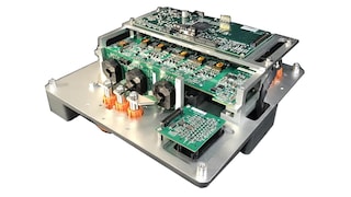
Ultra-Reliable MPC5777C MCU for Automotive and Industrial Engine Management
Advanced High Voltage Isolated Gate Driver for IGBT and SiC MOSFETs
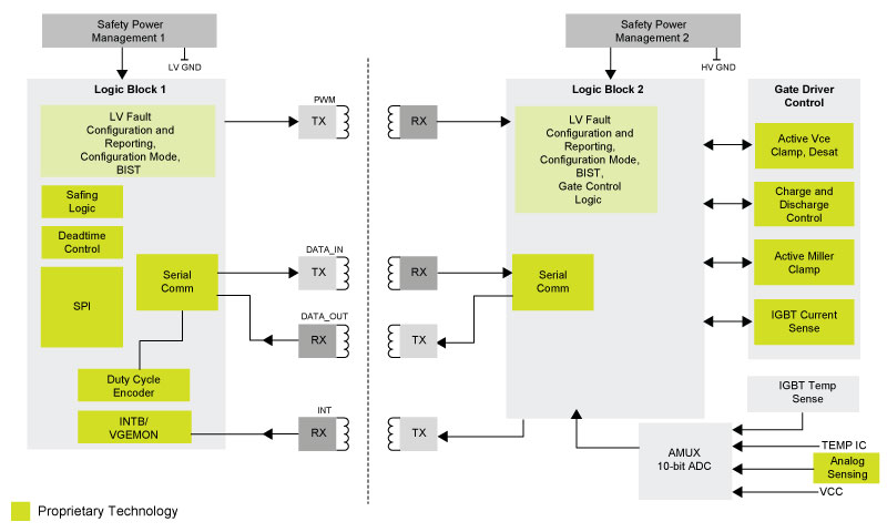
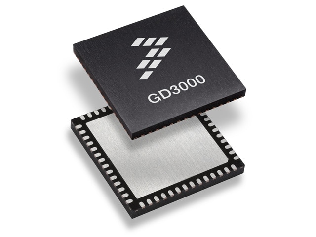
The GD3100 is an advanced single-channel gate driver for IGBTs/SiC. Integrated Galvanic isolation and low on-resistance drive transistors provide high charging and discharging current, low dynamic saturation voltage and rail-to-rail gate voltage control.
- Current and temperature sense minimizes IGBT/SiC stress during faults
- Accurate and configurable under voltage lockout provides protection while ensuring sufficient gate drive voltage headroom
- Autonomously manages severe faults and reports faults and status via INTB pin and an SPI interface. It is capable of directly driving gates of many IGBTs/SiC
- Self-test, control and protection functions are included for the design of high-reliability systems
製品詳細
ブロック図
Features
Key Features
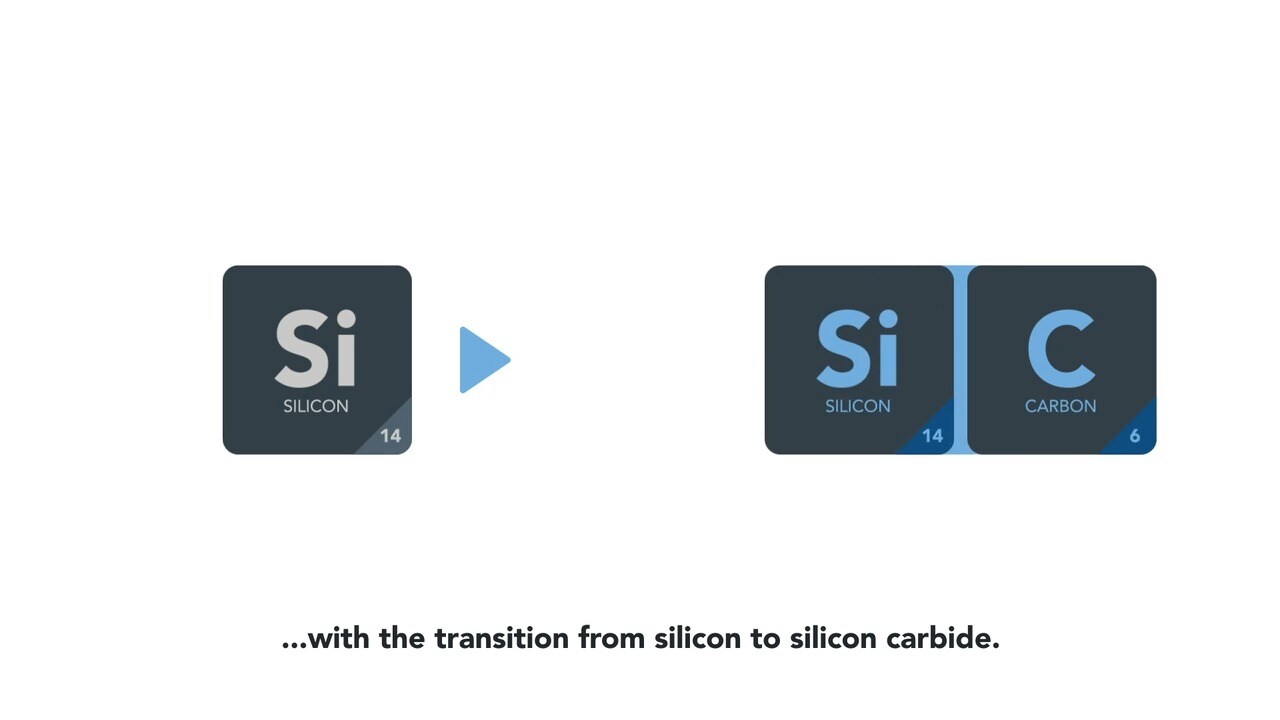
- HV isolated IGBT and SiC single gate driver IC device functions
- Load current 15 A (IL)
- Single channel
- Drain-to-source on resistance 500 mOhm RDS(ON)
- Load supply voltage min. -12 V, max. 25 V
- Supply voltage min. 5.6 V, max. 40 V
- Amient operating temperature -40 to 125 °C
- PWM and SPI interface and input controllers
High Level of Integration and Flexibility for Any IGBT/SiC Module
- Galvanic signal isolation
- 10 A on/off power stage
- Active Miller Clamp
- 3.3 or 5.0 V I/O
- Compatible with 200 to 1700 V IGBTs/SiC
- SPI for programmability and diagnostics
- Reduces BOM costs and PCB size
Fast Overcurrent or Short Circuit Protection
- Both I-sense or DESAT sense available
- Two-level turn-off
- Soft shutdown
Compliant with ISO26262 ASIL C/D Functional Safety Requirements (Certification Pending)
- VGE monitoring to verify communication between PWM input and Gate output
- Fail-safe pins allowing redundant gate control
- Secure SPI settings with Cycle Redundancy Check (CRC)
- Enforced deadtime protection
- Built-In Self-Test (BIST) for analog and digital circuits
部品番号: MC33GD3100A3EK, MC33GD3100B3EK, MC33GD3100BEK, MC33GD3100EK, MGD3100AM38EK, MGD3100AM58EK, MGD3100BM58EK, MGD3100BM38EK.
SafeAssure Functional Safety Program
When it comes to functional safety, NXP stands for quality and reliability. Our SafeAssure program simplifies
system-level safety requirements in accordance with ISO 26262.
Read more
関連製品
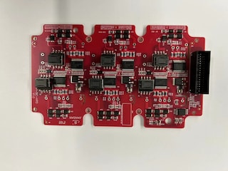
3-Phase Brushless Motor Pre-Driver
設計・リソース


ソフトウェア
クイック・リファレンス ソフトウェア・タイプ.
2 ソフトウェア・ファイル
-
デバッグと可視化ツール
FlexGUI for GD3100 and GD3160 Advanced Gate Driver Evaluation Software
注: より快適にご利用いただくために、ソフトウェアのダウンロードはデスクトップで行うことを推奨します。
トレーニング
6 トレーニング
-
オンデマンドウェビナー
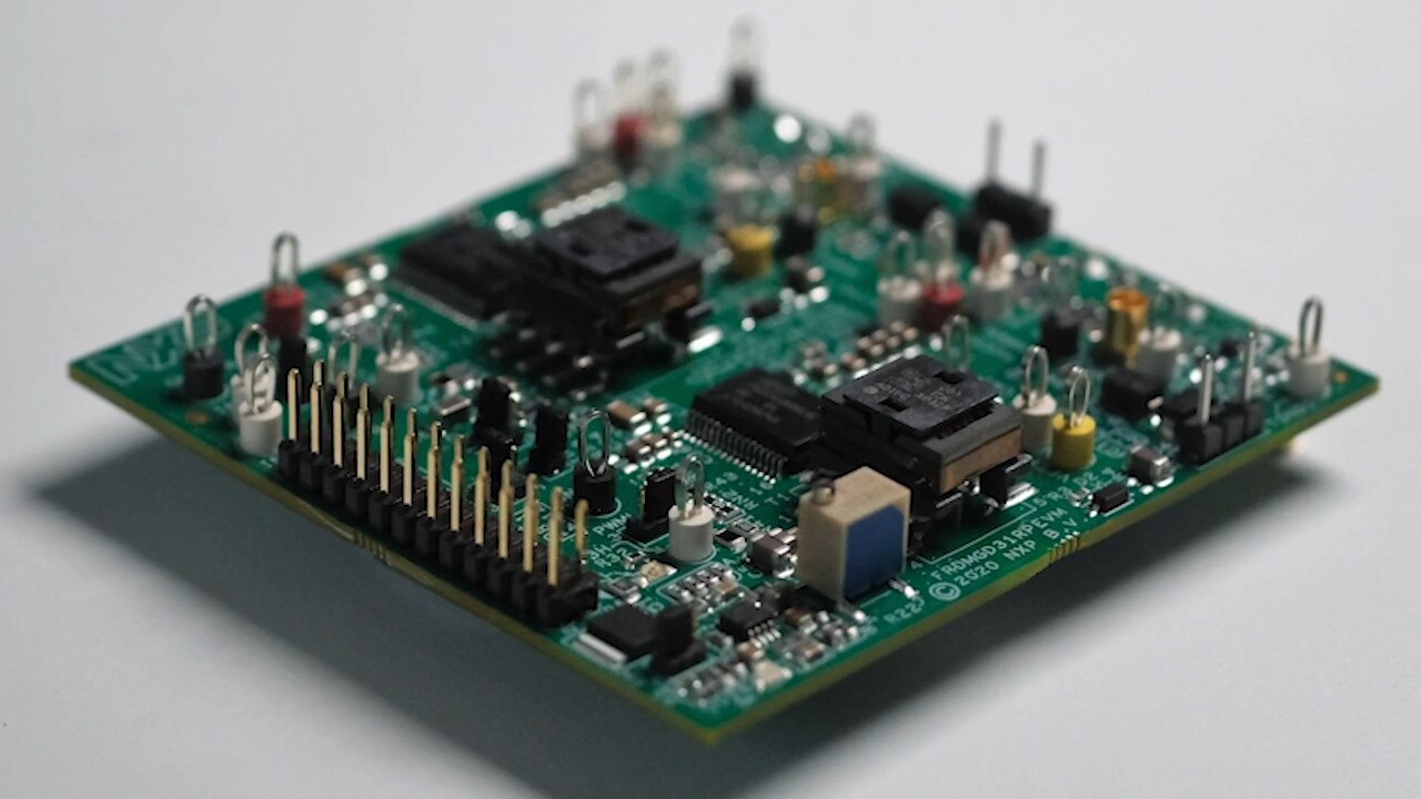
Getting Started with FRDM-GD3100HBIEVM Board
-
オンデマンドウェビナー
SiC EV Inverter Reference Design
-
オンデマンドウェビナー
Future Trends for HV Inverters