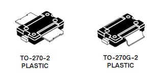
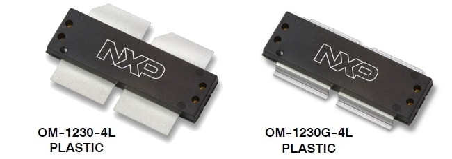
1.8-600 MHz, 1250 W CW, 50 V Wideband RF Power LDMOS Transistors

  • 新規採用非推奨
  • \n Contact support,\n your local sales representative or an\n \n NXP Authorized Distributor\n \n for product availability.\n

製品画像を見る

製品詳細

セクションを選択:

Features

  • Unmatched Input and Output Allowing Wide Frequency Range Utilization
  • Device can be used Single-Ended or in a Push-Pull Configuration
  • Qualified Up to a Maximum of 50 VDD Operation
  • Characterized from 30 to 50 V for Extended Power Range
  • Suitable for Linear Application with Appropriate Biasing
  • Integrated ESD Protection with Greater Negative Gate-Source Voltage Range for Improved Class C Operation
  • Characterized with Series Equivalent Large-Signal Impedance Parameters
  • RoHS Compliant
  • Recommended drivers: AFT05MS004N (4 W) or MRFE6VS25N (25 W)
  • Broadcast
    • FM broadcast
    • HF and VHF broadcast
  • Industrial, Scientific, Medical (ISM)
    • CO2 laser generation
    • Plasma etching
    • Particle accelerators (synchrotrons)
    • MRI
    • Industrial heating/welding
  • Aerospace
    • VHF omnidirectional range (VOR)
    • Weather radar
  • Mobile Radio
    • HF and VHF communications
    • PMR base stations

RF Performance Tables

Typical Performance

VDD = 50 Vdc

Load Mismatch/Ruggedness

1. Measured in 87.5-108 MHz broadband reference circuit.
2. The values shown are the center band performance numbers across the indicated frequency range.
3. Measured in 230 MHz narrowband test circuit.

ドキュメンテーション

クイック・リファレンス ドキュメンテーションの種類.

5 ドキュメント

設計・リソース

セクションを選択:

設計・ファイル

1-5 の 10 設計・ファイル

  • シミュレーションとモデル

    RF High Power Model ADS Model Kit goto: Click the Download button to select.

  • シミュレーションとモデル

    MRFE6VP61K25N RF High-Power Model AWR Product Model Design Kit

  • シミュレーションとモデル

    MRFE6VP61K25N S-Parameters

  • シミュレーションとモデル

    MRFE6VP61K25N RF High-Power Model ADS Product Model Design Kit

  • プリント基板と回路図

    MRFE6VP61K25N 87.5-108 MHz PCB DXF file

全て表示

サポート

お困りのことは何ですか??