デザイン・ファイル
1 設計・ファイル
-
シンボルおよびフットプリント
PCA9509GM-XQFN8U-CAD Symbol and PCB Footprint – BXL File
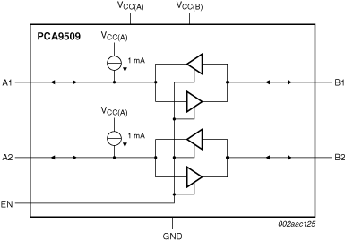
The PCA9509 is a level translating I2C-bus/SMBus repeater that enables processor low voltage 2-wire serial bus to interface with standard I2C-bus or SMBus I/O. While retaining all the operating modes and features of the I2C-bus system during the level shifts, it also permits extension of the I2C-bus by providing bidirectional buffering for both the data (SDA) and the clock (SCL) lines, thus enabling the I2C-bus or SMBus maximum capacitance of 400 pF on the higher voltage side. Port A allows a voltage range from 1.35 V to VCC(B) ‑ 1.0 V and requires no external pull-up resistors due to the internal current source. Port B allows a voltage range from 3.0 V to 5.5 V and is overvoltage tolerant. Both port A and port B SDA and SCL pins are high-impedance when the PCA9509 is unpowered.
For applications where Port A VCC(A) is less than 1.35 V or Port B VCC(B) is less than 3.0 V, use drop-in replacement PCA9509A.
The bus port B drivers are compliant with SMBus I/O levels, while port A uses a current sensing mechanism to detect the input or output LOW signal which prevents bus lock-up. Port A uses a 1 mA current source for pull-up and a 200 Ω pull-down driver. This results in a LOW on the port A accommodating smaller voltage swings. The output pull-down on the port A internal buffer LOW is set for approximately 0.2 V, while the input threshold of the internal buffer is set about 50 mV lower than that of the output voltage LOW. When the port A I/O is driven LOW internally, the LOW is not recognized as a LOW by the input. This prevents a lock-up condition from occurring. The output pull-down on the port B drives a hard LOW and the input level is set at 0.3 of SMBus or I2C-bus voltage level which enables port B to connect to any other I2C-bus devices or buffer.
The PCA9509 drivers are not enabled unless VCC(A) is above 0.8 V and VCC(B) is above 2.5 V. The enable (EN) pin can also be used to turn on and turn off the drivers under system control. Caution should be observed to change only the state of the EN pin when the bus is idle.
図を選択する。:
部品番号: PCA9509DP, PCA9509GM.
1 設計・ファイル
NXPから直接サポートを受けるには、以下のサイトをご覧ください。 エンジニアリング・サービス.
2 エンジニアリング・サービス

本製品をサポートするパートナーの一覧は、 パートナーマーケットプレイス.