
長期製品供給
対象製品には最低10年間の製品供給サポートが適用されます。自動車、通信、医療の各セグメント向けに開発された指定対象製品については、最低15年間の製品供給が保証されます。
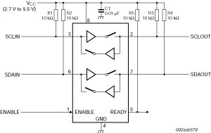
PCA9511Aは、ホットスワップ対応I²CバスおよびSMBusバッファで、データ・バスやクロック・バスを破損させることなく、通電中のバックプレーンへのI/Oカードの挿入を可能にします。制御回路により、カード上でバスが競合することなくバックプレーンに停止コマンドまたはバスのアイドル状態が発生するまでの間、バックプレーンがカードに接続されるのを防ぎます。接続が確立されると、PCA9511Aは双方向バッファリングを行い、バックプレーンとカードの静電容量を絶縁します。
PCA9511Aの立上がり時間アクセラレータ回路は、より弱いDCプルアップ電流を使用して、立上がり時間の要件を満たすことができます。PCA9511AはデジタルENABLE入力ピンを備え、このピンがHIGHにアサートされるとデバイスを有効化し、LOWのときは強制的に低電流モードにします。また、オープン・ドレインのREADY出力ピンにより、バックプレーン側とカード側が互いに接続されている (HIGH) か、接続されていない (LOW) かを示します。
挿入時には、PCA9511AのSDAおよびSCLラインが1 Vにプリチャージされ、チップの寄生容量の充電に必要な電流が最小限に抑えられます。
対象製品には最低10年間の製品供給サポートが適用されます。自動車、通信、医療の各セグメント向けに開発された指定対象製品については、最低15年間の製品供給が保証されます。
|
|
|
|
|
|
|
|---|---|---|---|---|---|
|
|
|
|
|
|
|
|
|
|
|
|
|
|
|
|
|
|
|
|
|
|
|
|
|
|
|
|
|
|
|
|
|
|
|
|
|
|
|
|
|
|
|
|
|
|
|
|
|
|
|
|
|
|
|
|
|
|
|
|
|
|
|
|
|
|
|
|
|
|
クイック・リファレンス ドキュメンテーションの種類
1-10 件/全 14 ドキュメント
コンパクトリスト
NXPから直接サポートを受けるには、以下のサイトをご覧ください。 エンジニアリング・サービス.
2 エンジニアリング・サービス

この製品をサポートするその他のパートナー製品を見つけるには、当社の Web サイトにアクセスしてください パートナーマーケットプレイス.