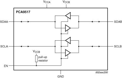
The PCA9517 is a CMOS integrated circuit that provides level shifting between low voltage (down to 0.9 V) and higher voltage (2.7 V to 5.5 V) I2C-bus or SMBus applications. While retaining all the operating modes and features of the I2C-bus system during the level shifts, it also permits extension of the I2C-bus by providing bidirectional buffering for both the data (SDA) and the clock (SCL) lines, thus enabling two buses of 400 pF. Using the PCA9517 enables the system designer to isolate two halves of a bus for both voltage and capacitance. The SDA and SCL pins are over voltage tolerant and are high-impedance when the PCA9517 is unpowered.
The 2.7 V to 5.5 V bus B-side drivers behave much like the drivers on the PCA9515A device, while the adjustable voltage bus A-side drivers drive more current and eliminate the static offset voltage. This results in a LOW on the B-side translating into a nearly 0 V LOW on the A-side which accommodates smaller voltage swings of lower voltage logic.
The static offset design of the B-side PCA9517 I/O drivers prevent them from being connected to another device that has rise time accelerator including the PCA9510, PCA9511, PCA9512, PCA9513, PCA9514, PCA9515A, PCA9516A, PCA9517 (B-side), or PCA9518. The A-side of two or more PCA9517s can be connected together, however, to allow a star topography with the A-side on the common bus, and the A-side can be connected directly to any other buffer with static or dynamic offset voltage. Multiple PCA9517s can be connected in series, A-side to B-side, with no build-up in offset voltage with only time of flight delays to consider.
The PCA9517 drivers are not enabled unless VCCA is above 0.8 V and VCC is above 2.5 V. The EN pin can also be used to turn the drivers on and off under system control. Caution should be observed to only change the state of the enable pin when the bus is idle.
The output pull-down on the B-side internal buffer LOW is set for approximately 0.5 V, while the input threshold of the internal buffer is set about 70 mV lower (0.43 V). When the B-side I/O is driven LOW internally, the LOW is not recognized as a LOW by the input. This prevents a lock-up condition from occurring. The output pull-down on the A-side drives a hard LOW and the input level is set at 0.3VCCA to accommodate the need for a lower LOW level in systems where the low voltage side supply voltage is as low as 0.9 V.