KITVR249SKTEVM評価ボードのスタート・ガイド
このドキュメントの内容
-
パッケージの内容
-
ハードウェアの入手
-
接続
サインイン 進行状況を保存するには アカウントをお持ちでない方 アカウントを作成する。
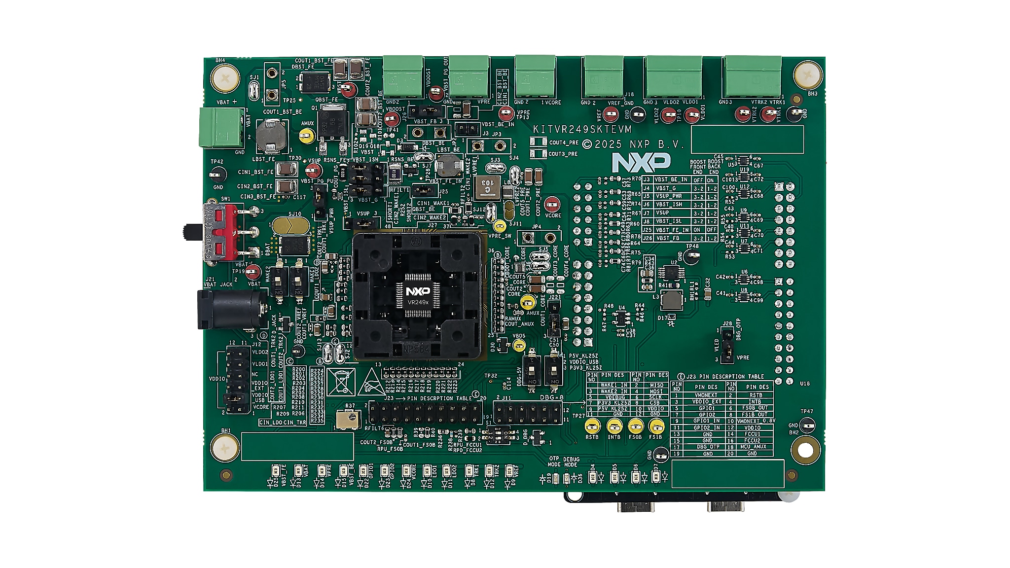
お客様の KITVR249SKTEVM
1. パッケージの内容
KITVR249SKTEVMキットでは、複数のスイッチング電源 (SMPS) および低ドロップアウト・レギュレータ (LDO) とともにVR249フェイルセーフ・パワー・マネジメント集積回路 (PMIC) を使用したプログラミング・ボードを評価、設計、実装、検証できます。プログラミング・ボードにはLQFP48パッケージ用のソケットが備えられ、さまざまなサンプルの機能テストとプログラミングが可能です。
このページでは、ハードウェアの接続、ソフトウェア/ツールのインストール、環境の構成など、キットを使用してKITVR249SKTEVMプログラミング・ボードを評価する方法について説明します。
1.1 キットの内容と同梱物一覧
キットには以下のものが含まれています。
- KITVR249SKTEVM
- 組立ておよびテスト済み評価ボードとプログラム済みFRDM-KL25Zマイクロコントローラ・ボード(静電気防止バッグ入り)
- 3.0フィートのUSB-STD-A to USB-C-miniケーブル
- 2ポジションのターミナル・ブロック・プラグ・コネクタ(ストレート、3.81 mm)x 2
- 3ポジションのターミナル・ブロック・プラグ・コネクタ(ストレート、3.81 mm)x 3
- ボードに搭載されたジャンパ
1.2 追加ハードウェア
このボードの作業をする際は、キットの内容物のほかに以下のハードウェアが必要になるか、または使用すると役立ちます。
- 電圧範囲8.0 V~40 V、電流制限1.0 A(初期値)の電源
1.3 最小システム要件
ボードの評価にはWindows PCワークステーションが必要です。最適な結果を得るには、PCに以下のものが装備されていることを確認してください。
- USB接続
- Windows 7、Windows 10、またはWindows 11オペレーティング・システム
1.4 ソフトウェア
評価ボードを操作する前に、ソフトウェア、特にNXPグラフィカル・ユーザー・インターフェース (GUI) をインストールする必要があります。このソフトウェアは、KITVR249SKTEVMページにあります。
2. ハードウェアの入手
2.1 ボードの特長
KITVR249SKTEVM評価ボードには、以下のものが含まれます。
- バッテリー電圧 (VBAT) 電源コネクタ(ジャックおよびPhoenix)
- LQFP48(Low-profile Quad Flat Package、48ピン)用のバーンイン・オープントップ・ソケット
- プリレギュレータ電圧 (VPRE) 出力:3.7 V~6.35 V
- 独立モードまたはフロントエンド・トポロジでの昇圧電圧 (VBOOST) によりバッテリー・クランキング・プロファイルをサポート
- コア電圧 (VCORE) 出力:0.8 V~3.35 V、最大1.65 A
- 低ドロップアウト・レギュレータ1 (LDO1) および低ドロップアウト・レギュレータ2 (LDO2):3.3 Vまたは5.0 V、最大400 mA
- トラッキング電圧レギュレータ1 (VTRK1) およびトラッキング電圧レギュレータ2 (VTRK2):3.3 Vまたは5.0 V、最大150 mA
- 外部ADコンバータ (ADC) リファレンス用の電圧リファレンス (VREF) 高精度レギュレータ
- フェイルセーフ出力0 (FS0B) およびフェイルセーフ出力1 (FS1B):外部セーフティ・ピン
- ソフトウェアGUIへの接続を容易にするUSB to SPIプロトコル
- 信号またはレギュレータの状態を示すLED
- ワンタイム・プログラマブル (OTP) ヒューズの手動または自動プログラミング
- アナログ・マルチプレクサ (AMUX) または外部ADCによる高度なシステム監視
- 外部電圧モニタ (VMON) をテストするためのアナログ可変抵抗
2.2 ボードの説明
KITVR249SKTEVMキットは柔軟に活用でき、デバイスのすべての機能を実行し、アプリケーションの主要部分の測定を行うことができます。ボードに接続されたFRDM-KL25ZとVR249 NXP GUIソフトウェアを組み合わせることで、VR249 PMICの完全な設定と制御を実現します。ボード上のLQFP48ソケットにより、さまざまなサンプルのテストやプログラミングが可能です。
OTPプログラミング、エミュレーション、または評価を行うには、VR249 PMICのサンプルをソケットに挿入する必要があります。完全なデバイス評価に向けてはボードの性能が制限されているため、目的に応じて別の評価ボードや構成が必要かどうかを確認してください。
2.3 ボードのコンポーネント
このセクションでは、ボードのコンポーネントについて説明します。図1は、ボード上の重要なコンポーネントを示しています。
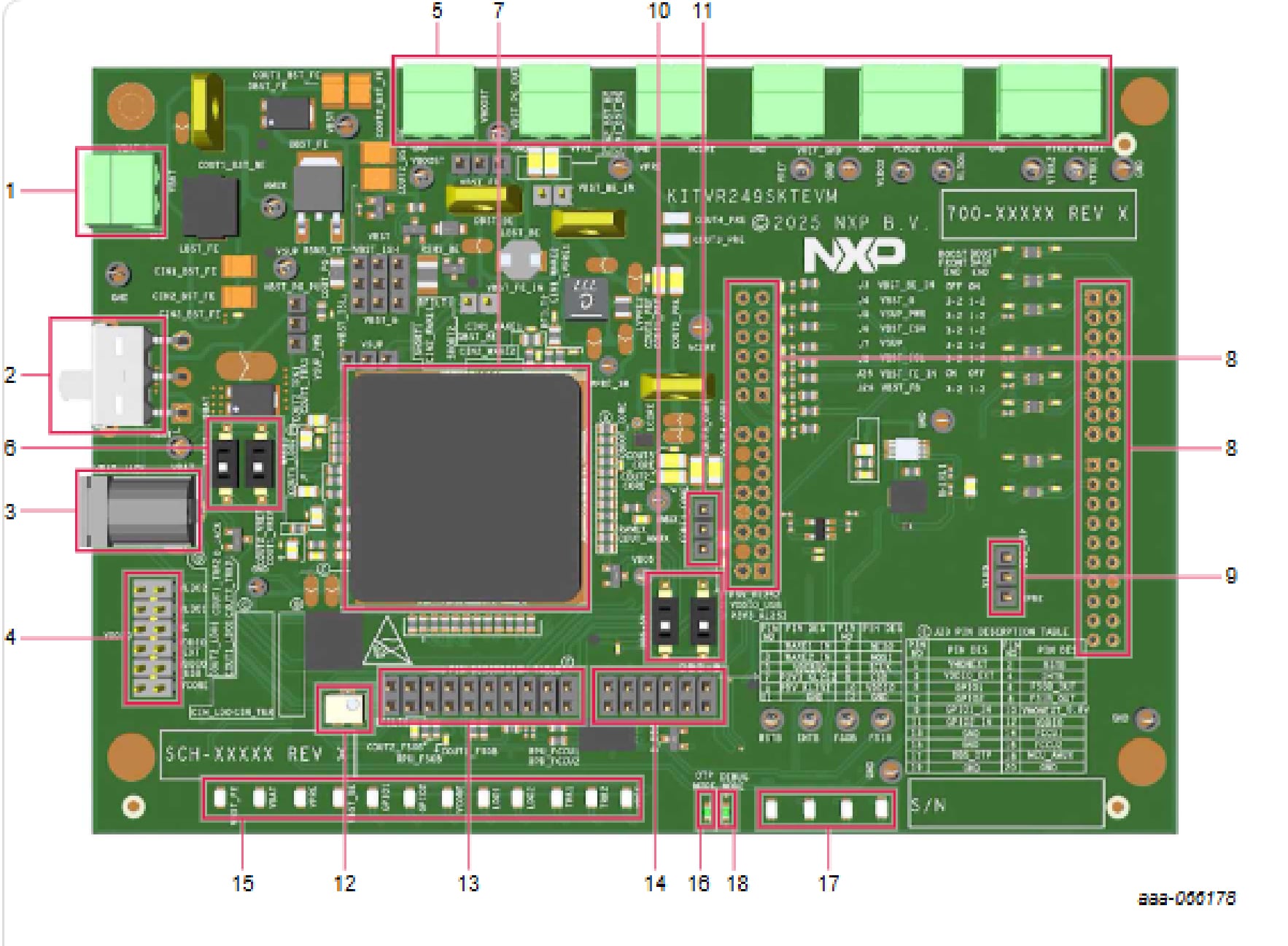
以下に示すリストの各項目は、上の図の番号に対応しています。
- VBAT Phoenixコネクタ
- VBAT 3ポジション・スイッチ
- VBATジャック・コネクタ
- VDDIO選択
- レギュレータ出力
- WAKE1およびWAKE2入力スイッチ
- LQFP48ソケット
- KL25Z Freedomヘッダ(裏面)
- DEBUGピン電圧ソース選択(スイッチまたはMCU)
- DEBUGピン電圧レベル・スイッチ
- VDDIO USB電圧レベル選択
- VMONEXT可変抵抗器
- 信号コネクタ
- プログラミング・コネクタ
- レギュレータ出力LEDインジケータ
- プログラム書き込み電圧LEDインジケータ
- セーフティ出力LEDインジケータ
- デバッグ・モードLEDインジケータ
3. 接続
3.1 接続
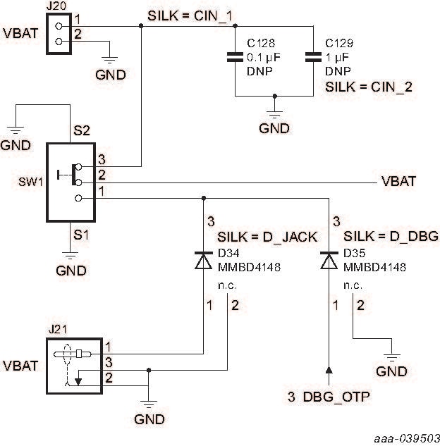
KITVR249SKTEVMボードの電源は、PhoenixコネクタJ20またはジャック・コネクタJ21を介して供給できます。3ポジション・スイッチSW1を使用して、アクティブな電源コネクタを選択します。公称VBAT電圧は24 Vで、最大40 Vをサポートします。下の図2は、関連する回路図を示しています。公称VBAT電圧は24 Vで、最大40 Vをサポートします。
| 回路図ラベル | 信号名 | 説明 |
|---|---|---|
J20-1 |
VBAT | バッテリー電圧供給入力 |
J20-2 |
GND | グランド |
| 回路図ラベル | 信号名 | 説明 |
|---|---|---|
SW1ピン2-3 |
VBAT | Phoenixコネクタからボードに電源供給 |
SW1ピン2(中央ポジション) |
VBAT | ボードに電源供給なし |
SW1ピン2-1 |
VBATジャック | ジャック・コネクタからボードに電源供給 |
キットは、図3に示すデフォルトのジャンパ設定で提供されます。この設定は、フロントエンドの昇圧トポロジに適しています。
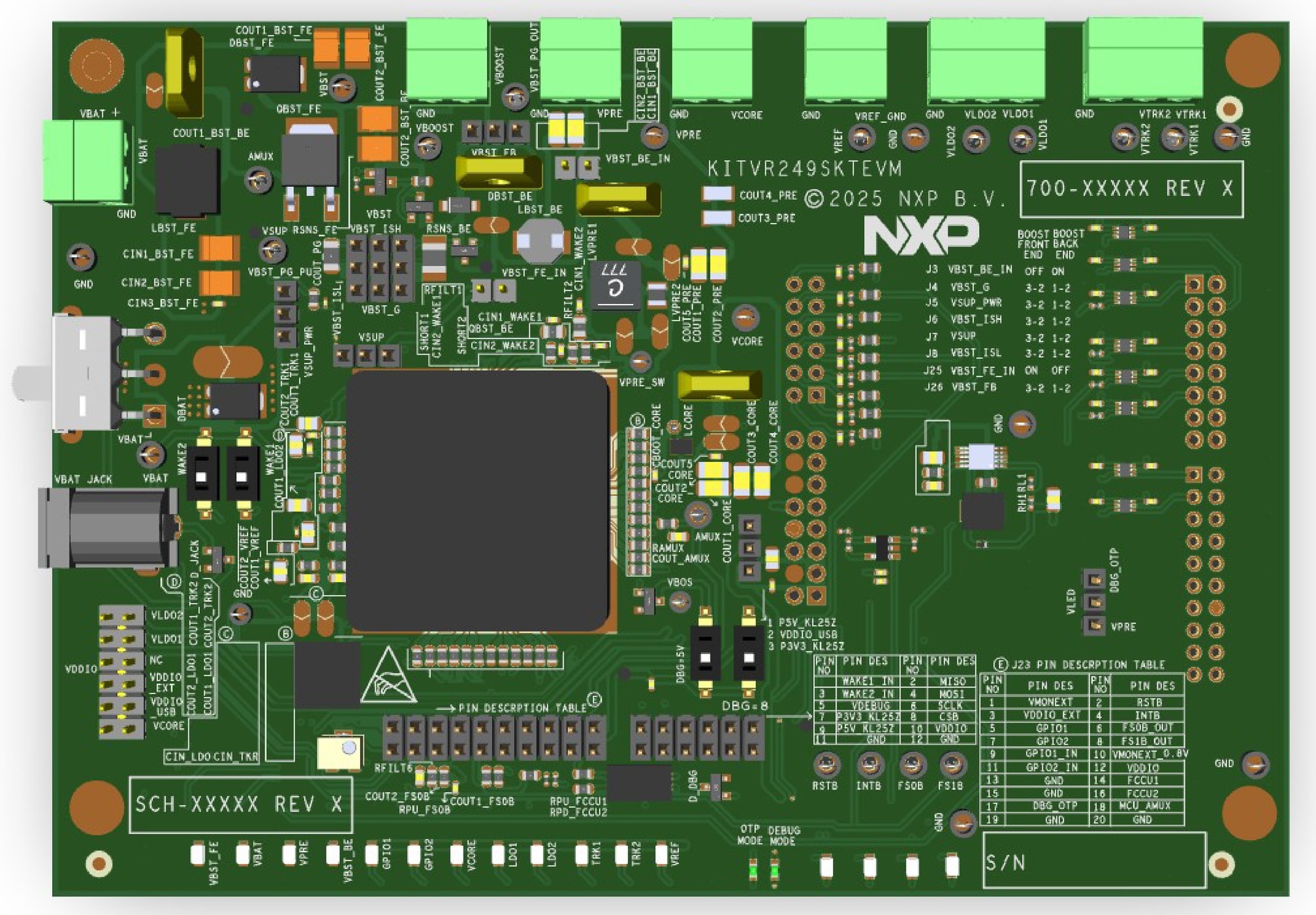
| 回路図ラベル | 信号名 | デフォルト設定 |
|---|---|---|
J51 |
VBST_BE_IN | オフ |
J49 |
VBST_G | 3-2 |
J50 |
VSUP_PWR | オン |
J53 |
VBST_ISH | 3-2 |
J48 |
VSUP | 3-2 |
J55 |
VBST_ISL | 3-2 |
J52 |
VBAT_D | 3-2 |
J54 |
VBST_FB | 3-2 |
J12 |
VDDIO | VDDIO_USB |
J28 |
VLED | 3-2 |
J22 |
VDDIO_USB | 3-2 |
SW2 |
WAKE1 | オフ |
SW3 |
WAKE2 | オフ |
SW6 |
DBG = 5 V | オフ |
SW7 |
DBG = 8 V | オフ |