アプリケーション・ノート (8)
-
PN5190 LPCD and ULPCD[AN14931]
-
Crystal Oscillator Design Guide[AN14518]
-
PN5190 design-in recommendations[AN12551]
-
PN5190 questions and answers[AN13669]
-
PN5190 antenna design guide[AN12549]
-
PN5190 EMV L1 SW porting to IMX1170[AN13425]
カタログ (1)
データ・シート (2)
-
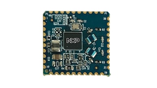
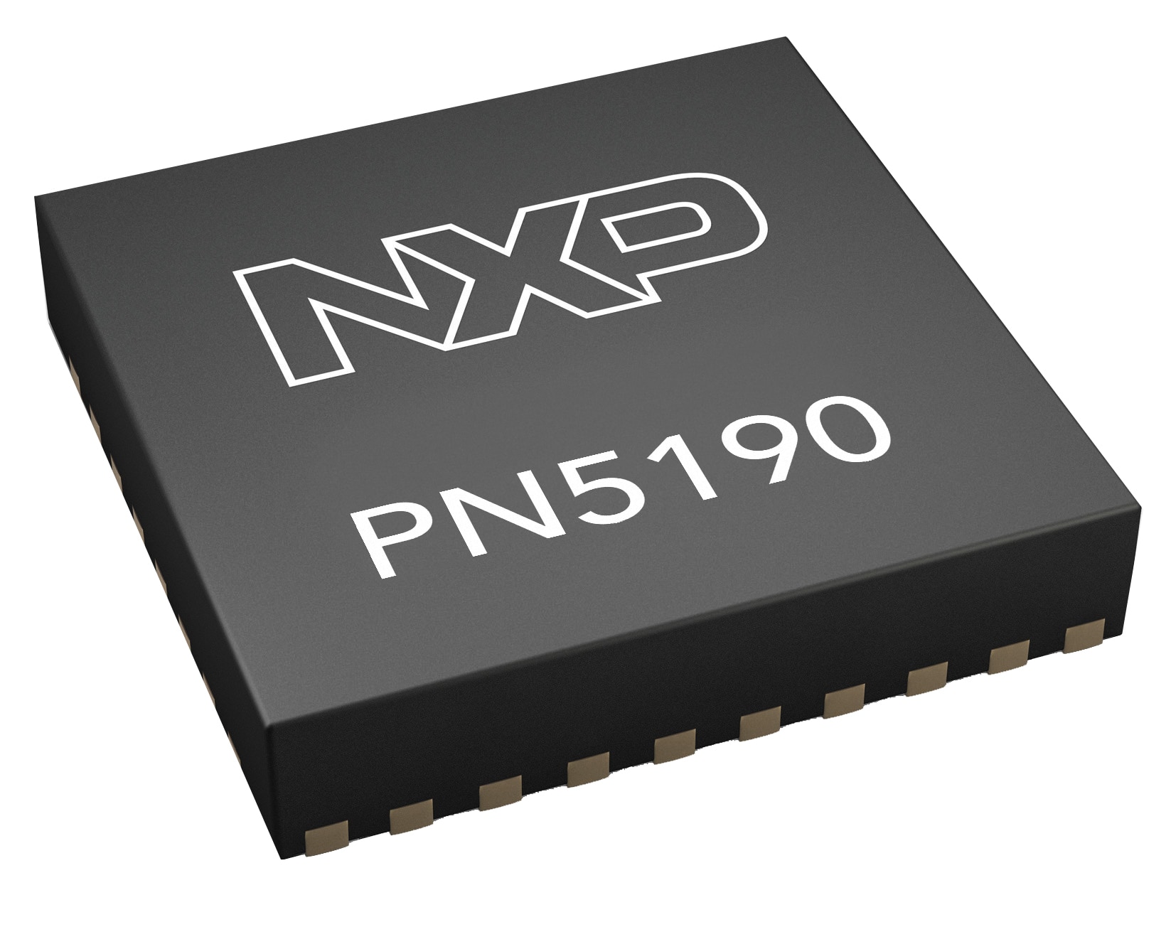
PN5190B2 NFC Frontend[PN5190B2]