
-
OM17005
-
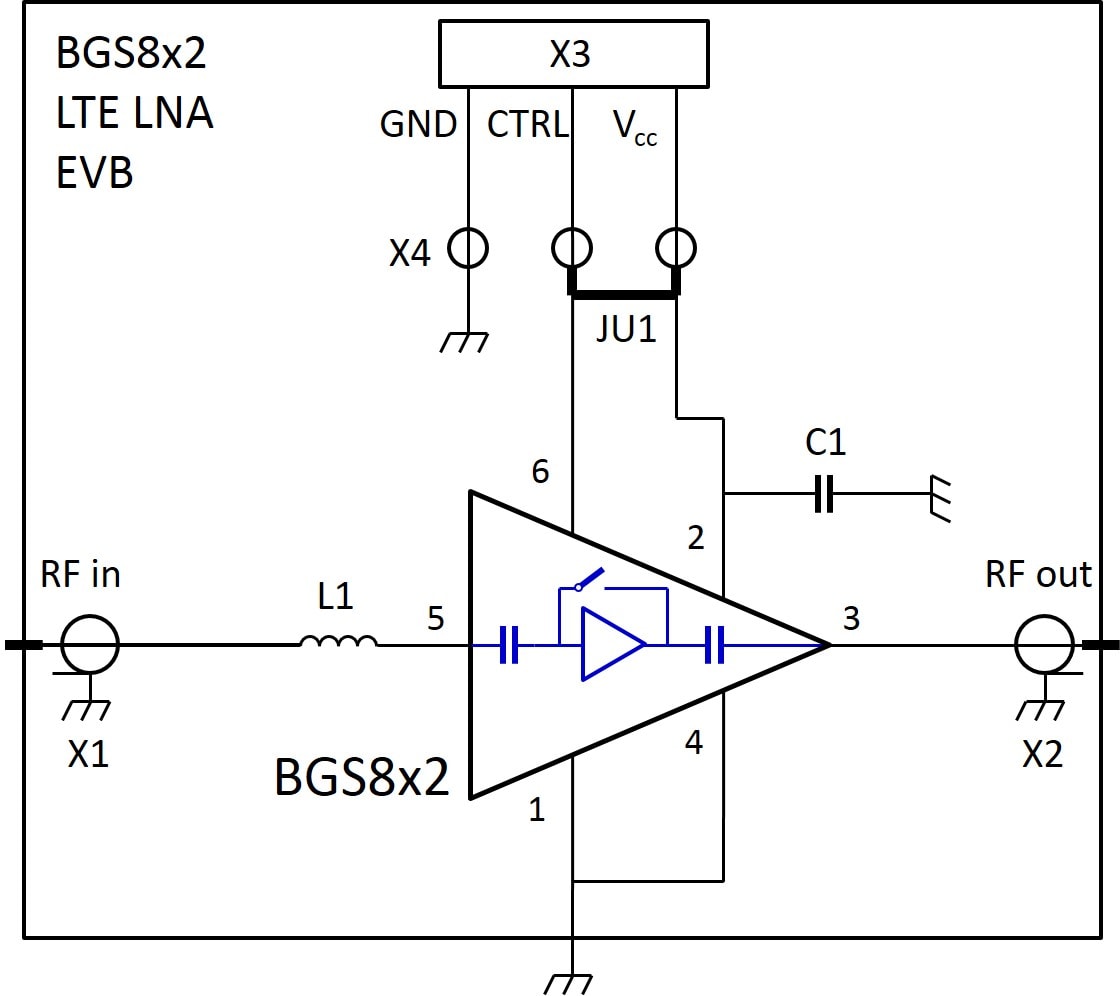
BGS8L2 LTE LNA with bypass switch evaluation board.
The BGS8L2 LTE LNA evaluation board simplifies the evaluation of the BGS8L2 LNA for the LTE application. The evaluation board enables testing of the device performance and requires no additional support circuitry. The board is fully assembled with the BGS8L2, the input series inductor and a decoupling capacitor. The board is supplied with two SMA connectors for input and output connection to RF test equipment. The BGS8L2 can operate from a 1.5 V to 3.1 V single supply and consumes about 5.2 mA.