S32E2 Safe and Secure High-Performance Real-Time Processors with Actuation Support
High Voltage PMIC with Multiple SMPS
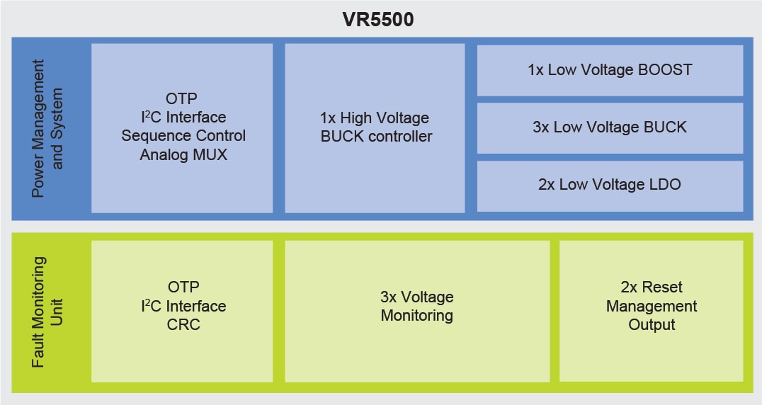
The VR55 is an automotive high voltage multi-output power supply integrated circuit, with focus on radio, telematics and infotainment applications. It includes multiple switch mode and linear voltage regulators.
This PMIC is part of a complete family of devices offering scalability in power and safety FS84 (ASIL B) and FS85 (ASIL D), pin to pin and software compatible.
製品詳細
Features
Key Features
- 60 V maximum input voltage for automotive and truck markets
- Multiple SMPS and LDO
- Standby OFF mode with very low sleep current (10 µA)
- Device control via I2C interface with CRC
- Three voltage monitoring circuits, dedicated interface for MCU monitoring, power good, reset and interrupt outputs
- QM, AEC-Q100 rev H qualified
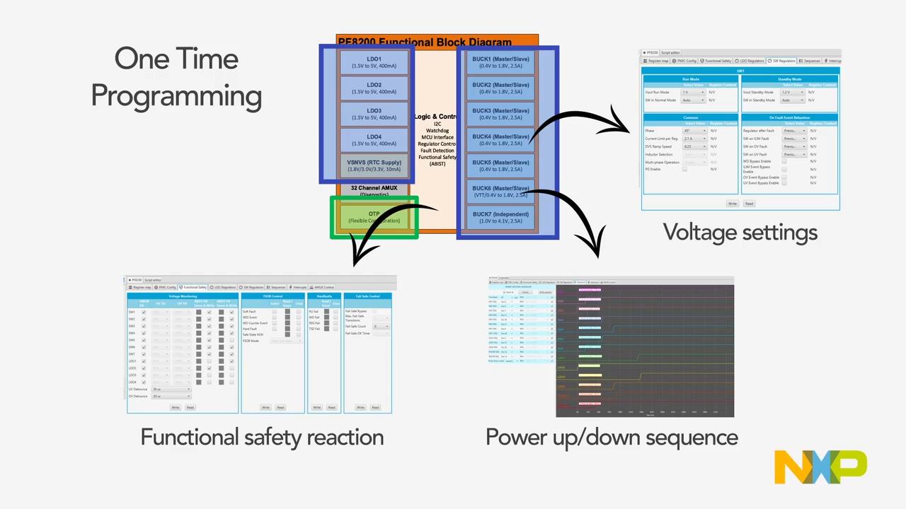
Programmability
- Supplies, sequencing, and specific functions can be programmed by One Time programmable (OTP) memory
- Standard Predefined OTP supporting popular MCU can be found in data sheet under “ordering information” chapter
- During development phase, Customized OTP part can be programmed using the KITVR55-FSSKTEVM board
- Custom OTP can be provided for production. Please contact your NXP sales channel (NXP or your distributor)
- Custom OTP form can be downloaded OTP Configuration Tool
部品番号: MC33VR5500V0ES, MC33VR5500V1ES.
比較表
Scalable Power and Safety Concept
| Part number | Buck 1 | Buck 2 | Buck 3 | Vpre | Boost | Safety level |
|---|---|---|---|---|---|---|
| VR5500 | 0.8 V - 1.8 V 2.5 A Multi-phase and SVS option |
12 / 24 V HV BUCK - 10 A |
5 V - 5.74 V 1.5 A peak |
Quality Mgt (QM) | ||
| FS8400 | N/A | N/A | Fit for ASIL B | |||
| FS8500 | Fit for ASIL D | |||||
| FS5502 | 1.0 V - 4.1 V 3.6 A peak |
N/A | Quality Mgt (QM) | |||
| FS8410 | 5 V - 5.74 V 1.5 A peak |
Fit for ASIL B | ||||
| FS8510 | Fit for ASIL D | |||||
| FS8420 | 0.8 V - 1.8 V 2.5 A Multi-phase and SVS option |
N/A | Fit for ASIL B | |||
| FS8520 | Fit for ASIL D | |||||
| FS8430 | 1.0 V - 3.3 V 2.5 A |
Fit for ASIL B | ||||
| FS8530 | Fit for ASIL D | |||||
| FS6600 | Fit for ASIL D |
BYLink System Power Platform
This platform facilitates the design of safe power management systems thanks to a portfolio of configurable and linkable devices. It simplifies complex power supply
subsystems into a single smart solution.
Learn more about this platform
関連製品
High Voltage PMIC with Multiple SMPS and LDO, Primary Companion Chip for S32Rx
設計・リソース
ソフトウェア
クイック・リファレンス ソフトウェア・タイプ.
1 ソフトウェア・ファイル
-
スニペット、ブート・コード、ヘッダ、モニタなど
VR5500 OTP Configuration tool
注: より快適にご利用いただくために、ソフトウェアのダウンロードはデスクトップで行うことを推奨します。