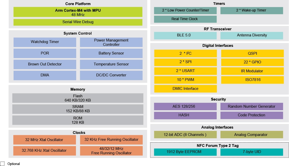
The QN9090 and QN9030 are the latest microcontrollers in the QN series of Bluetooth low energy devices that achieve ultra-low-power consumption and integrate an Arm®Cortex®-M4 CPU with a
comprehensive mix of analog and digital peripherals. With support for up to 640KB onboard flash and 152 KB SRAM, the memory integration provides room and flexibility for complex applications and
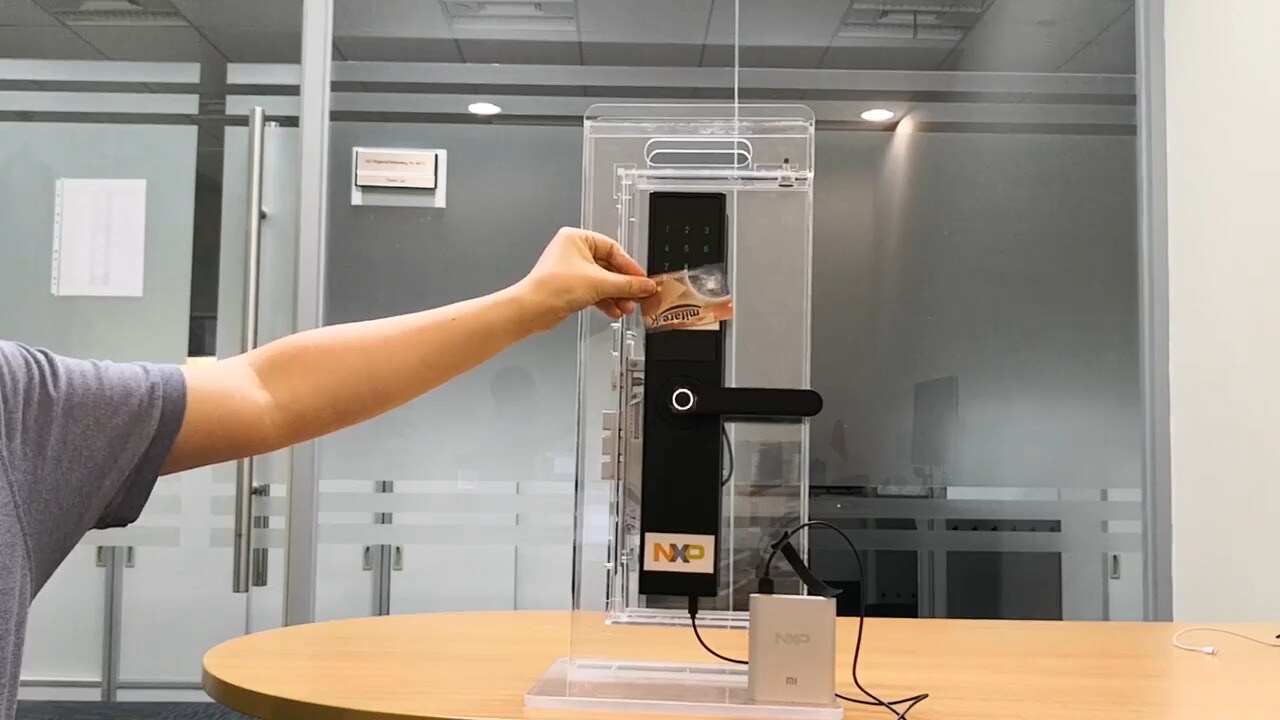
safe Over-the-Air (OTA) updates. QN series devices have a rich set of MCU peripherals including multiple serial communication interfaces. Within the QN series the QN9090T and QN9030T integrate NFC
NTAG to support use cases such as out-of-band pairing. By tapping a device based on the QN9090T with an NFC reader device, such as a smart phone or tablet, a Bluetooth LE connection can be
established quickly simplifying the pairing process.