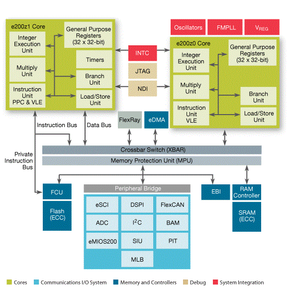
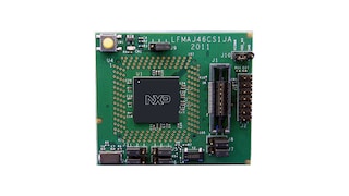
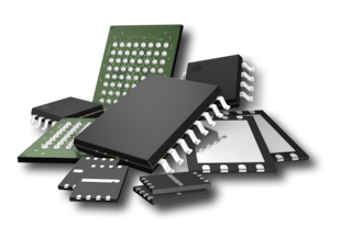
Designed for body electronics, the NXP® MPC5510 MCU belongs to an expanding family of automotive-focused products that address the next wave of central body and gateway applications within the vehicle.
- Offers high-performance while continuing to meet low-power requirements
- Enables centralized architectures, which reduce the number of distributed ECUs and complexity of vehicle architectures
- Provides extensive communication capabilities (e.g., FlexRay, multiple CAN and LIN support)
- Offers room to grow with scalable family ranging from 512 KB up to 1.5 MB of embedded flash
- Backed by a third-party ecosystem of development tools and software