アプリケーション・ノート (5)
カタログ (1)
データ・シート (1)
パッケージ情報 (1)
ユーザ・ガイド (1)
-
LPC3130/31 User manual[UM10314]
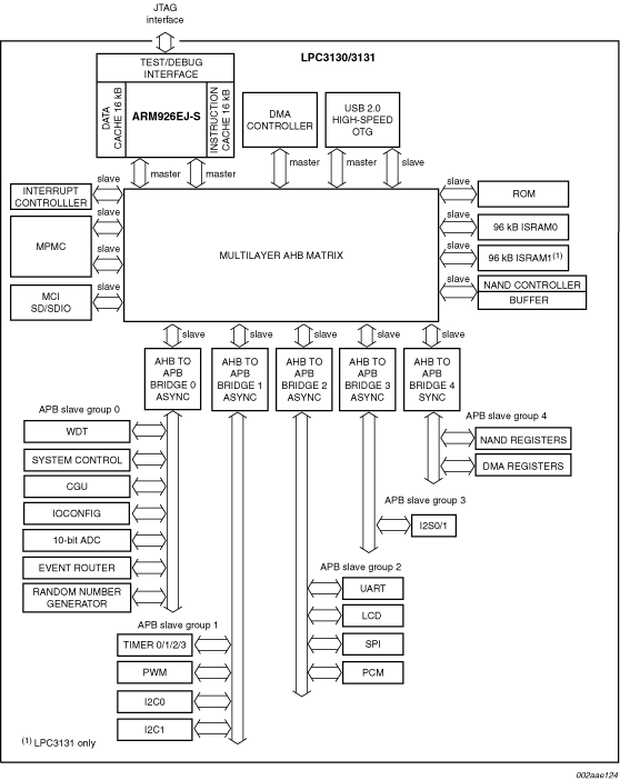
The NXP® LPC3130/3131 combine an 180 MHz ARM926EJ-S CPU core, high-speed USB 2.0 On-The-Go (OTG), up to 192 KB SRAM, NAND flash controller, flexible external bus interface, four channel 10-bit ADC, and a myriad of serial and parallel interfaces in a single chip targeted at consumer, industrial, medical, and communication markets. To optimize system power consumption, the LPC3130/3131 have multiple power domains and a very flexible Clock Generation Unit (CGU) that provides dynamic clock gating and scaling.
|
|
|
|
|
|
|
|---|---|---|---|---|---|
|
|
|
|
|
|
|
|
|
|
|
|
|
|
|
|
|
|
|
|
|
|
|
|
|
|
|
|
|
|
|
|
|
|
|
|
|
|
|
|
|
|
|
|
|
|
|
|
|
|
|
|
|
|
|
|
|
|
|
|
|
|
|
|
|
|
|
|
|
|
クイック・リファレンス ドキュメンテーションの種類
9 ドキュメント
コンパクトリスト
2 設計・ファイル
完全な内訳を受け取ります。 製品の設置面積などについては、 eCad ファイル.