長期製品供給
対象製品には最低10年間の製品供給サポートが適用されます。自動車、通信、医療の各セグメント向けに開発された指定対象製品については、最低15年間の製品供給が保証されます。
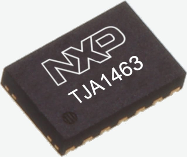
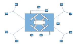
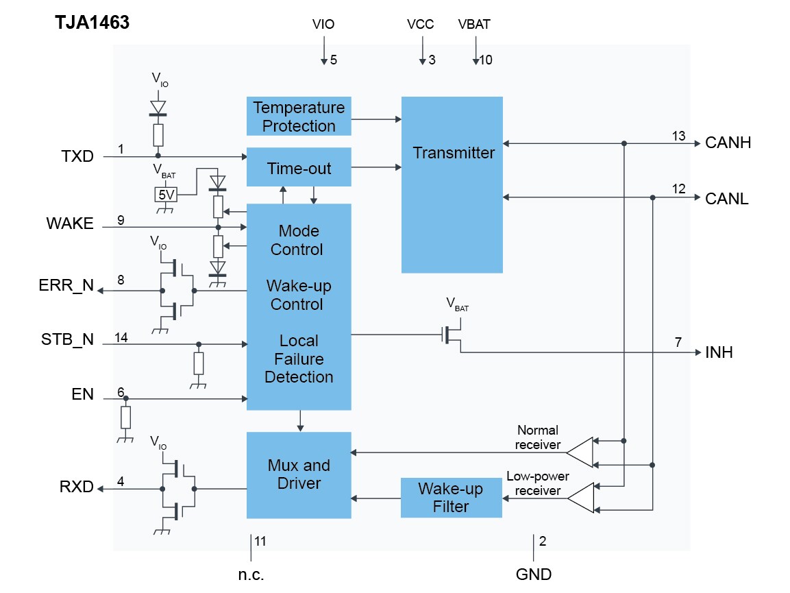
TJA1463は、TJA146xトランシーバ・ファミリに属するスリープ・モード付きのCANシグナル改善機能(Signal Improvement Capability:SIC)トランシーバです。ISO 11898-2:2024で定義されるCAN SICを備えています。TJA1463は、ISO 11898-2:2024およびSAE J2284-(1-5) で定義されるCAN物理層の要件を満たし、高速の従来型CANおよびCAN FDと完全に相互運用可能です。
CANシグナル改善により、ネットワーク上の信号リンギングが大幅に低減され、より大規模なトポロジ内で信頼性の高いCAN FD通信を5 Mbit/sで実行できます。また、ビット・タイミングの対称性が大幅に向上し、最大8 Mbit/sのCAN FD通信を可能にします。
TJA1463は下位互換性を備え、NXP TJA1043やTJA1443などの従来型CANおよびCAN FDトランシーバをドロップインで置き換えることができます。
対象製品には最低10年間の製品供給サポートが適用されます。自動車、通信、医療の各セグメント向けに開発された指定対象製品については、最低15年間の製品供給が保証されます。
|
|
|
|
|
|
|
|---|---|---|---|---|---|
|
|
|
|
|
|
|
|
|
|
|
|
|
|
|
|
|
|
|
|
|
|
|
|
|
|
|
|
|
|
|
|
|
|
|
|
|
|
|
|
|
|
|
|
|
|
|
|
|
|
|
|
|
|
|
|
|
|
|
|
|
|
|
|
|
|
|
|
|
|
完全な内訳を受け取ります。 製品の設置面積などについては、 eCad ファイル.
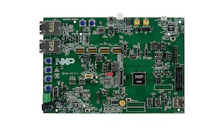
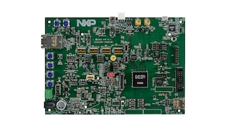
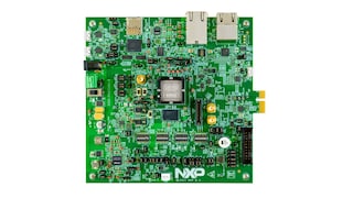
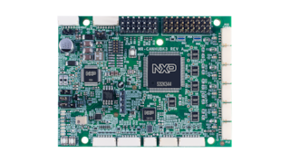
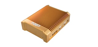
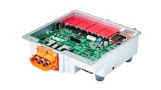
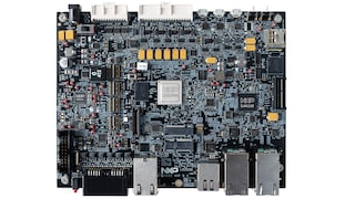
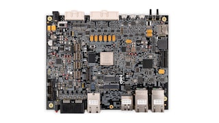
1-5 件/全 18 ハードウェア提供

NXPから直接サポートを受けるには、以下のサイトをご覧ください。 エンジニアリング・サービス.
3 エンジニアリング・サービス

この製品をサポートするその他のパートナー製品を見つけるには、当社の Web サイトにアクセスしてください パートナーマーケットプレイス.