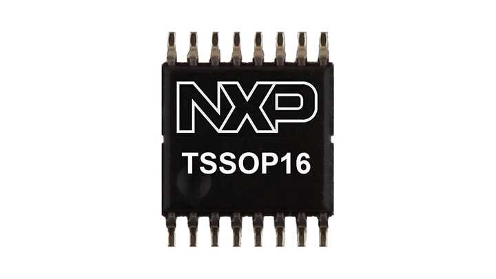
The NX3L4051 is a low-ohmic 8-channel analog switch, suitable for use as an analog or
digital multiplexer/demultiplexer. The NX3L4051 has three digital select inputs (S1 to S3),
eight independent inputs/outputs (Y0 to Y7) and a common input/output (Z). All eight
switches share an enable input (E). A HIGH on E causes all switches into the high
impedance OFF-state, independent of Sn.
Schmitt trigger action at the digital inputs makes the circuit tolerant to slower input rise and
fall times. Low threshold digital inputs allows this device to be driven by 1.8 V logic levels
in 3.3 V applications without significant increase in supply current ICC. This makes it
possible for the NX3L4051 to switch 4.3 V signals with a 1.8 V digital controller,
eliminating the need for logic level translation.The NX3L4051 allows signals with
amplitude up to VCC to be transmitted from Z to Yn or from Yn to Z. Its low ON resistance
(0.5 Ω) and flatness (0.13 Ω) ensures minimal attenuation and distortion of transmitted
signals.


