Flexis 32ビットColdFire® V1マイクロコントローラ
ハードウェア
クイック・リファレンス
ボードタイプ.
5 ハードウェア提供
-
 エミュレータ、プローブ、プログラマ
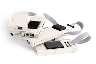
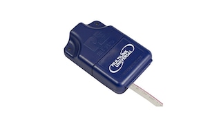
Universal Multilink開発インターフェース注目
アクティブ -
 エミュレータ、プローブ、プログラマ
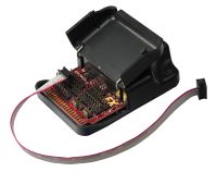
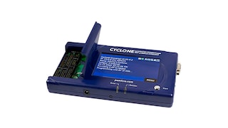
PEmicro Cyclone programmer
アクティブ -
 エミュレータ、プローブ、プログラマ
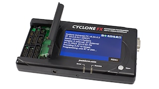
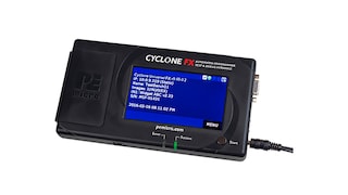
PEmicro Cyclone FX programmer
-
追加ハードウェアを利用可能 パートナー・ソリューションの特集を表示.
-
 エミュレータ、プローブ、プログラマ
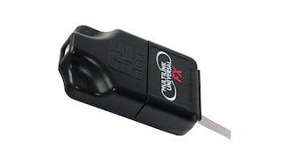
Universal Multilink FX高速開発インターフェース
アクティブ -
 評価・開発ボード
MCF51QE128 Demonstration Board
アクティブ