

Tiny Real-Time Clock/Calendar with Alarm Function, Battery Switch-Over, Time Stamp Input and I²C-Bus
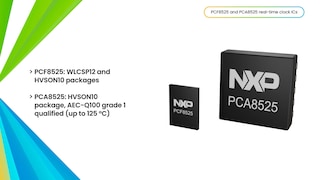
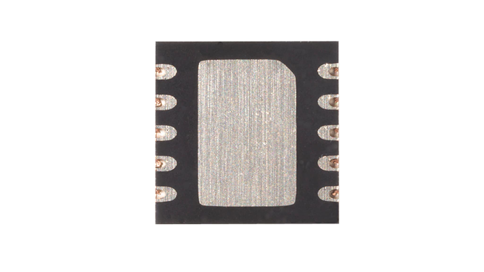
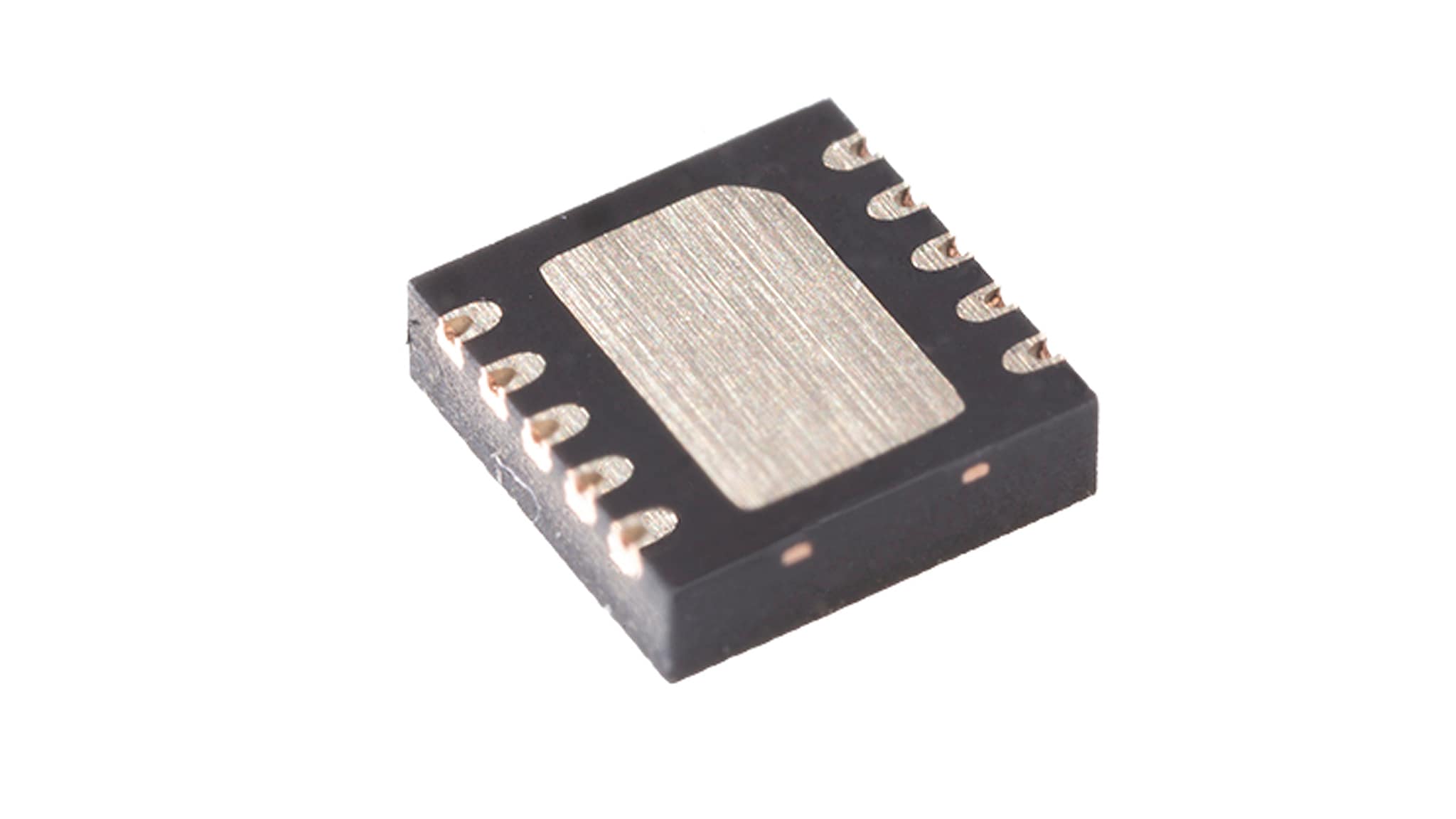
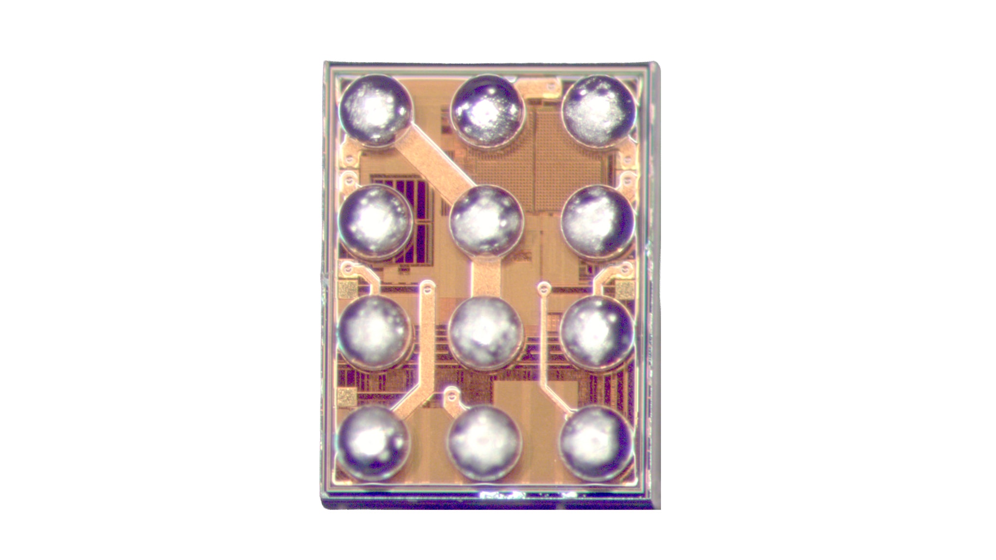
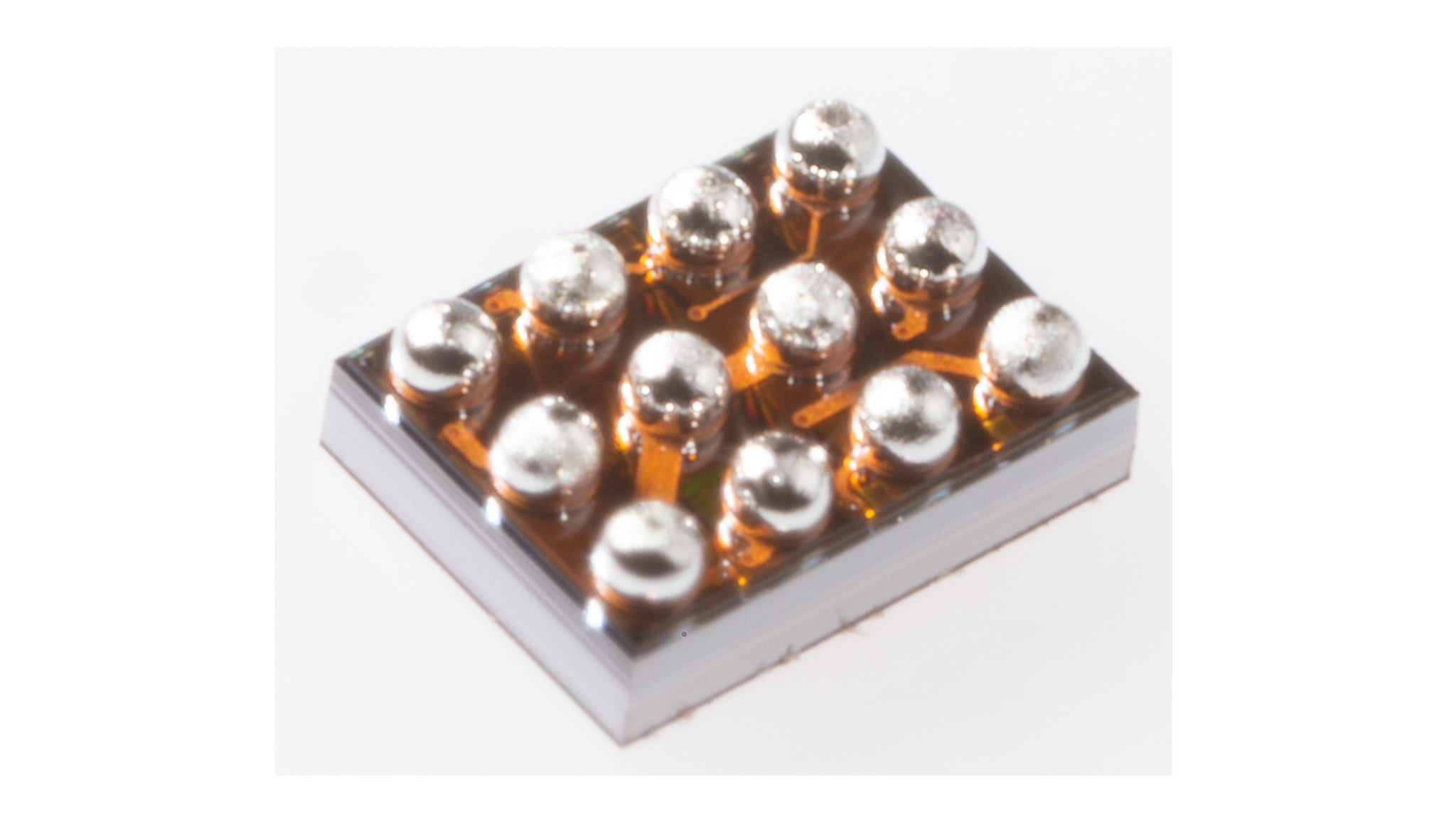
PCF8525は、正確な計時性能を提供するリアルタイム・クロック (RTC) ICです。HVSONバージョンは最大精度±30 ppmの温度補償を備え、他のRTC ICソリューションと比べて最大5倍の精度を提供します。WLCSPバージョンは補償を省略することで、スペースに制約のある設計向けに非常にコンパクトなフットプリントを達成しています。
Tiny Real-Time Clock/Calendar with Alarm Function, Battery Switch-Over, Time Stamp Input and I²C-Bus
クイック・リファレンス ドキュメンテーションの種類
4 ドキュメント
コンパクトリスト