S32K389EVB-Q437評価ボードのスタート・ガイド
このドキュメントの内容
-
パッケージの内容
-
ソフトウェアの入手
-
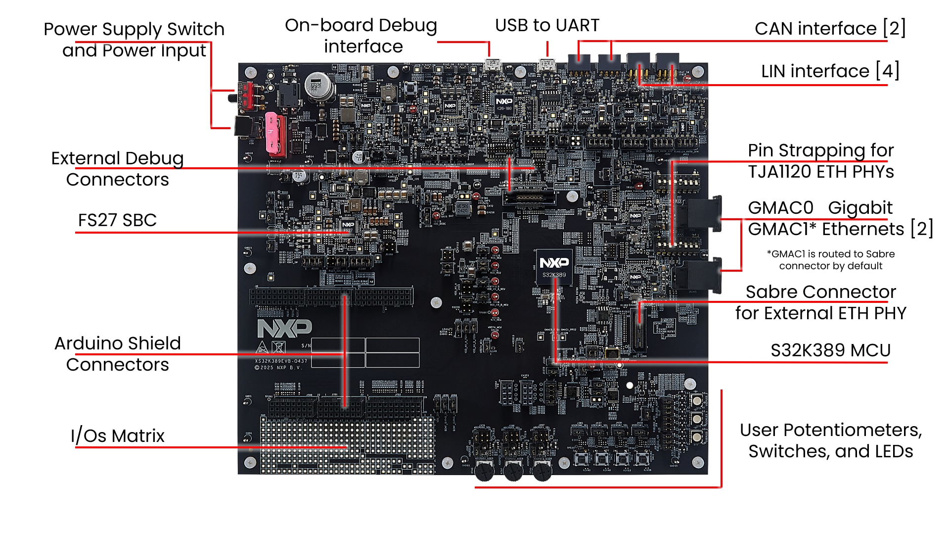
ハードウェアの構成
-
アプリケーションの作成
-
ビルドと実行
サインイン 進行状況を保存するには アカウントをお持ちでない方 アカウントを作成する。
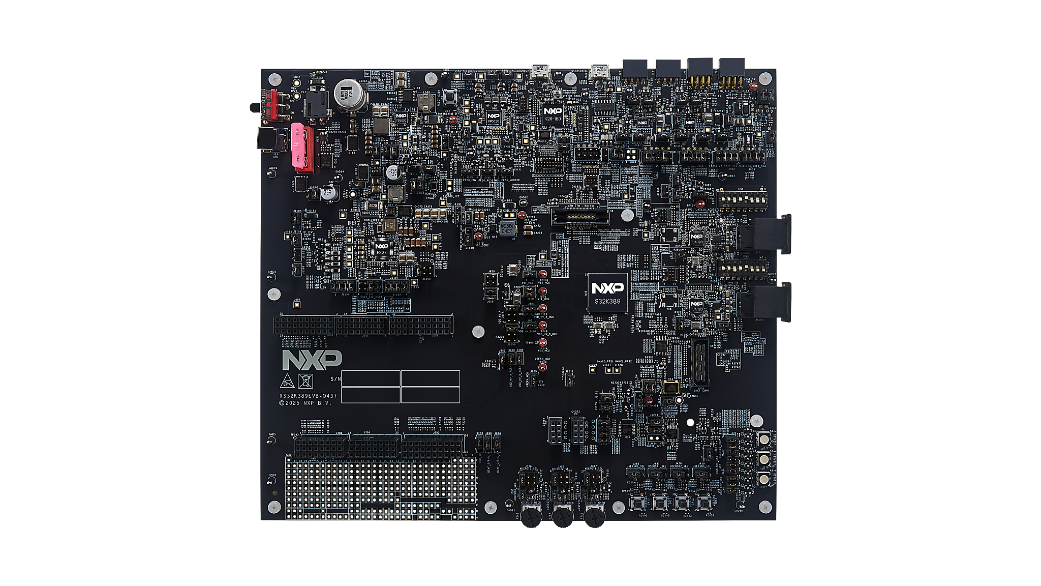
お客様の S32K389EVB-Q437 汎用車載用途向け評価ボード
1. パッケージの内容
1.1 S32K389EVB-Q437評価ボードについて

2. ソフトウェアの入手
資格情報を使用してnxp.comにサインインします。
ビデオをご覧いただくか、以下のステップ・バイ・ステップ・ガイドに従ってソフトウェアをインストールし、S32K389EVB-Q437評価ボードをセットアップしてください。
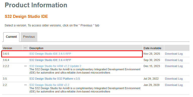
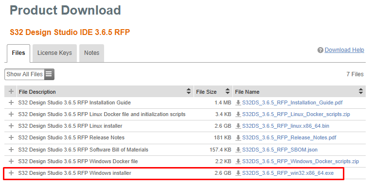
2.1 S32 Design Studio for S32 Platform IDEの入手
S32 Design Studio for S32 Platform 3.6.5をダウンロードしてインストールします。
2.2 GCC v10.2のインストール
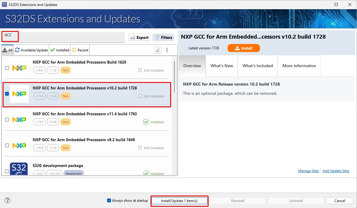
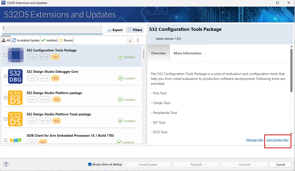
S32DSで、トップメニューから[Help(ヘルプ)]→[S32DS Extensions and Updates(S32DSの拡張と更新)]の順に進み、[S32DS Extensions and Updates(S32DSの拡張と更新)]ダイアログを開きます。
GCCバージョンv10.2をインストールします(使用されているリアルタイム・ドライバで必要)
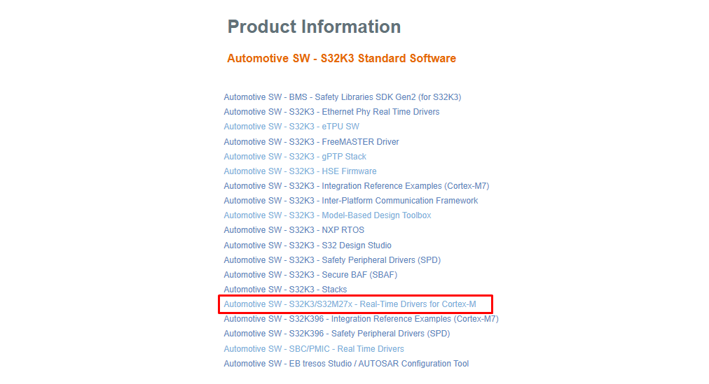
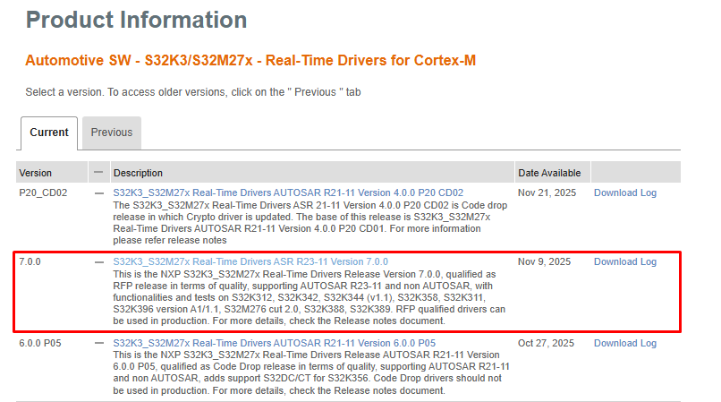
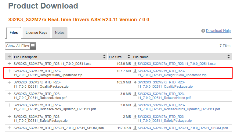
2.3 リアルタイム・ドライバ (RTD) のダウンロード
S32K3_S32M27x Real-Time Drivers ASR R23-11 Version 7.0.0 - 更新サイト・パッケージをダウンロードします
2.4 RTDドライバのインストール
S32DSで、トップメニューから[Help(ヘルプ)]→[S32DS Extensions and Updates(S32DSの拡張と更新)]の順に進み、[S32DS Extensions and Updates(S32DSの拡張と更新)]ダイアログを開きます。[Add Update Sites(更新サイトを追加)]をクリックし、ダウンロードしたRTD *.zipを参照します。オプションとして、ドラッグ&ドロップにより更新サイトをS32DSに追加することもできます。
S32K3 Real-Time Drivers ASR R23-11 Version 7.0.0を検索し、(すべてを)選択してインストールします。
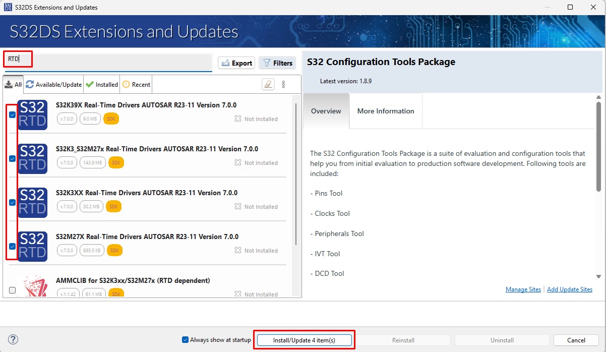
インストールが完了したら、S32DSを再起動します。
2.5 FreeMASTERランタイム・デバッグ・ツールの入手
S32K389EVB-Q437は、FreeMASTERランタイム・デバッグ・ツールを使用するとパフォーマンスが向上します。
FreeMASTERランタイム・デバッグ・ツールをダウンロードしてインストールします
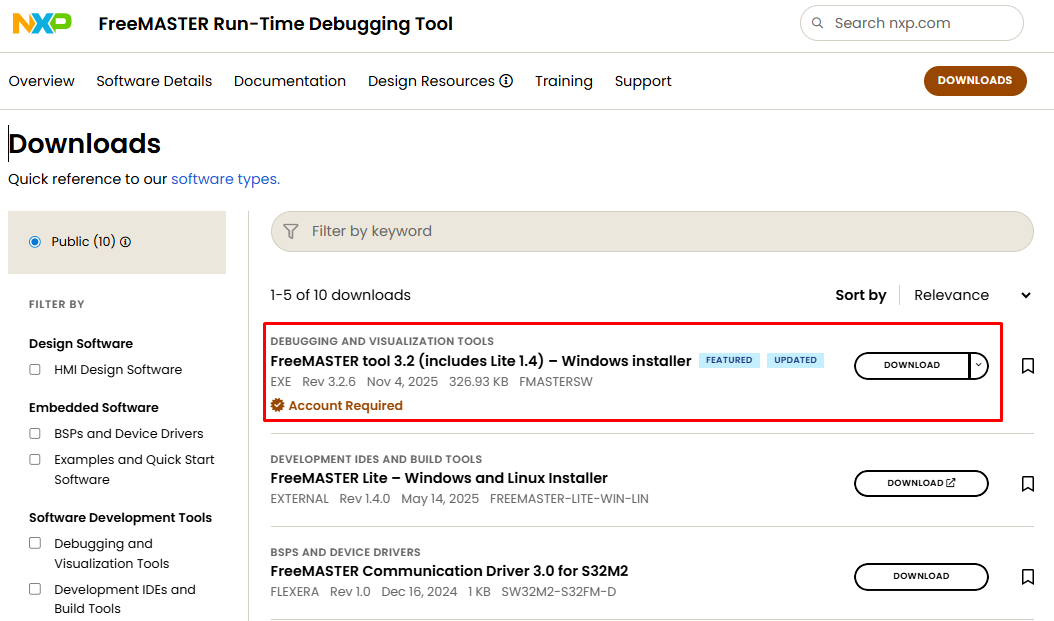
MCU側では、FreeMASTER通信ドライバが必要になります
S32DSで、トップメニューから[Help(ヘルプ)]→[S32DS Extensions and Updates(S32DSの拡張と更新)]の順に進み、[S32DS Extensions and Updates(S32DSの拡張と更新)]ダイアログを開きます。
FreeMASTER通信ドライバを選択してインストールします。
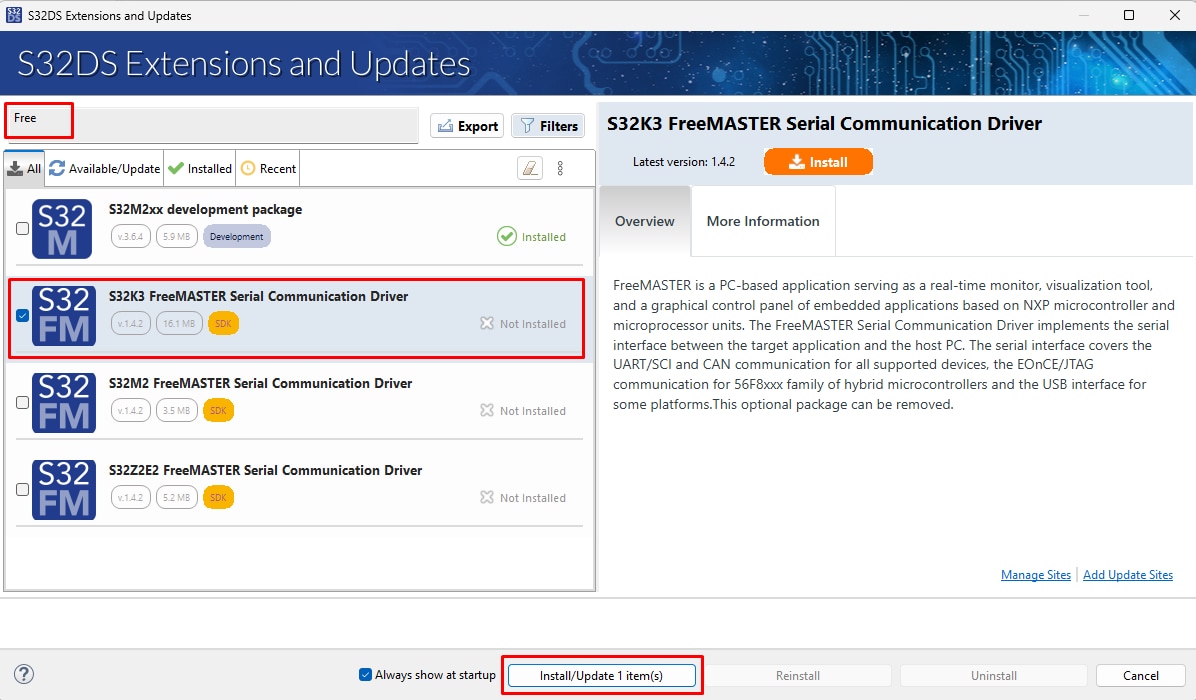
FreeMASTER通信ドライバをインストールします
インストールが完了したら、S32DSを再起動します。
3. ハードウェアの構成
3.1 ジャンパをデフォルト状態に設定
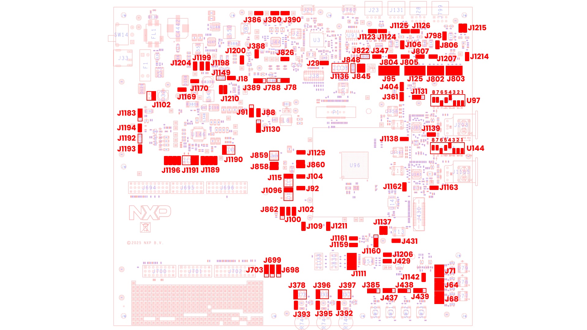
| ジャンパ | 状態 | 備考 | |
|---|---|---|---|
| VBAT入力 | J1102 |
1-2 | 過電圧保護、低電圧保護、逆接続保護をイネーブル。 |
J1214 |
閉 | 単方向電源スイッチU150の入力をイネーブル。 | |
J1215 |
1-3、2-4 | 単方向電源スイッチU150の入力と出力をそれぞれ接続。 | |
| FS27/SBC電源 | J1169 |
閉 | VBATをVBAT_FS27にルーティング。 |
J1170 |
閉 | VBAT_FS27をFS27インターフェースおよびVSUPドメインにルーティング。 | |
J1183 |
1-2 | FS27デバッグ・オプションの選択。FS27_VDEBUGをFS27_VBOSから派生。 | |
J1189 |
1-2、3-4、5-6、7-8 | FS27とMCU間のSPI接続 (LPSPI3)。 | |
J1190 |
1-2 | FS27 WAKE1をMCUのPTA8 (EXTWAKE) にルーティング。 | |
J1191 |
5-6、7-8 | FS27_RESETとFS27_WAKE2の両方をRESET_MCUにルーティング。 | |
J1192 |
開 | FS27_GPIO1信号 | |
J1193 |
閉 | FS27電圧ドメインLEDインジケータをイネーブル。 | |
J1194 |
閉 | FS27 GPIO2をMCUのPTA9 (PGOOD) にルーティング。 | |
J1196 |
1-2、3-4、5-6、7-8 | FS27 FS0BおよびFS1BをMCUに接続、FS27_FCCUからFCCU MCUへの信号間のFS27 FCCU接続。 | |
| FS5600 | J18 |
閉 | FS5600電圧ドメインLEDインジケータをイネーブル。 |
J1149 |
開 | RESET_MCUをFS5600 PGOOD信号から切断。 | |
J1198 |
閉 | プルアップ抵抗を使用してFS5600 EN1をFS27_VPREにルーティング。 | |
J1199 |
閉 | プルアップ抵抗を使用してFS5600 EN2をFS27_VPREにルーティング。 | |
J1200 |
閉 | P3V3SW_OUT1をFS5600 SW2スイッチング・レギュレータにルーティング - 3.3 V、10 A。 | |
J1204 |
閉 | P5V0SW_OUTをFS5600 SW1スイッチング・レギュレータにルーティング - 5 V、3 A。 | |
J1210 |
1-2、3-4 | FS5600のI²C信号をMCUに接続。 | |
| PF5020 | J78 |
1-2 | PF5020 OTPプログラミング入力電源電圧 = グランド。 |
J380 |
閉 | PF50_SW1OUT_1V2ジャンパが1.2 V出力をイネーブル。 | |
J386 |
閉 | PF50_SW1OUT_1V8ジャンパが1.8 V出力をイネーブル。 | |
J388 |
閉 | PF5020 VIN用のP5V0SW_OUT電源。 | |
J389 |
1-2 | PF5020出力がプルアップ経由で電源をイネーブル。 | |
J390 |
閉 | PF50_SW1OUT_1V1ジャンパが1.1 V出力をイネーブル。 | |
J788 |
開 | PF5020 RESETをRESET_MCU信号から切断。 | |
J826 |
閉 | PF5200電圧ドメインLEDインジケータをイネーブル。 | |
| S32K389 MCU電源 | J88 |
閉 | 入力電圧をMCUのVDD_DCDCに接続。 |
J91 |
1-2 | MCUのVDD_DCDCのソースとしてP3V3SW_OUT1を選択。 | |
J92 |
閉 | 選択されたVDD_HV_BとVDD_HV_B_MCU間の接続。 | |
J100 |
閉 | VDD_HV_AペリフェラルのVDD_HV_A_PERH電圧リファレンス。 | |
J102 |
閉 | VDD_HV_BペリフェラルのVDD_HV_B_PERH電圧リファレンス。 | |
J104 |
閉 | 選択されたVDD_HV_AとVDD_HV_A_MCU間の接続。 | |
J109 |
閉 | VDD_HV_A_MCUとVDD_VREFH_MCU間の接続。 | |
J115 |
1-2 | FS27_LDO1_OUTをVDD_HV_A、5 V出力に接続。 | |
J858 |
1-2、3-4 | FS27_VCOREをV15 MCUの1.5 V出力に接続。 | |
J859 |
開 | FS27_VCOREをV15_SMPSスイッチング・レギュレータから切断。 | |
J860 |
1-2、3-4 | V11 MCUの接続。このジャンパにより、V11の電源とMCU間の接続がイネーブルになります。 | |
J862 |
1-2 | VDD_REFH_MCUペリフェラルの電圧リファレンスをVDD_HV_Aから派生。 | |
J1096 |
1-2 | FS27_LDO2_OUTをVDD_HV_B、3.3 V出力に接続。 | |
J1129 |
閉 | V15 MCUの接続。このジャンパにより、V15の電源とMCU間の接続がイネーブルになります。 | |
J1130 |
1-2 | SMPSが必要でない場合、VDD_DCDCをVDD_HV_B_MCUに接続すること。 | |
| JTAG | J29 |
閉 | VDD_HV_A_PERHからVDD_SWD/JTAGへの電圧供給、JTAGインターフェースへの供給用。 |
J1211 |
閉 | RESET_MCU信号をMCU PTA5ピンに接続。 | |
| オンボード・デバッガ | J822 |
開 | VDD_HV_A_PERHによりVDDIO_SDAの電源をイネーブル。 |
J848 |
開 | RESET_MCU信号からのSDAリセットをディセーブル。 | |
J1136 |
開 | オンボード・デバッガJTAG信号をMCUから切断。 | |
| SABREコネクタ | J429 |
閉 | このジャンパにより、VDD_HV_A_PERHとVDD_HV_A_SABRE間の接続がイネーブルになります。 |
J431 |
閉 | P3V3_GMAC1からSABREコネクタへの電源をイネーブル。 | |
J1111 |
1-2、3-4、5-6、7-8 | MCUのLPSPI4信号をSABREコネクタに接続。 | |
J1137 |
1-2、3-4 | GMAC1 MDC機能をPTA28に接続、GMAC1 MDIO機能をPTA29に接続。 | |
J1206 |
閉 | MCUのLPSPI4 CS1信号をSABREコネクタに接続。 | |
| GMAC0 TJA1120_A | J361 |
閉 | 単方向電源スイッチU124の入力を接続。 |
J404 |
閉 | 単方向電源スイッチU124の入力をイネーブル。 | |
J1131 |
1-2 | 単方向電源スイッチU124の出力をバイパス。 | |
J1138 |
閉 | MCUのPTB4をTJA1120_Aの割込みピンに接続。 | |
J1139 |
閉 | MCUのPTD13をTJA1120_Aのウェイク・ピンに接続。 | |
J1142 |
閉 | MCUのPTG12をTJA1120_Aのリセット・ピンに接続。 | |
| U97-1 | + | GMAC0ピン・ストラッピングConfig0 - プルアップ。 | |
| U97-2 | + | GMAC0ピン・ストラッピングConfig1 - プルアップ。 | |
| U97-3 | + | GMAC0ピン・ストラッピングConfig2 - プルアップ。 | |
| U97-4 | - | GMAC0ピン・ストラッピングConfig3 - プルダウン。 | |
| U97-5 | 0 | GMAC0ピン・ストラッピングConfig4 - オープン。 | |
| U97-6 | + | GMAC0ピン・ストラッピングConfig5 - プルアップ。 | |
| U97-7 | 0 | GMAC0ピン・ストラッピングConfig6 - オープン。 | |
| U97-8 | 0 | GMAC0ピン・ストラッピングTJA1120_RST - オープン。 | |
| GMAC1 TJA1120_B | J1159 |
閉 | 単方向電源スイッチU142の入力を接続。 |
J1160 |
1-2 | 単方向電源スイッチU142の出力をバイパス。 | |
J1161 |
閉 | 単方向電源スイッチU142の入力をイネーブル。 | |
J1162 |
閉 | MCUのPTB26をTJA1120_Bの割込みピンに接続。 | |
J1163 |
閉 | MCUのPTA31をTJA1120_Bのウェイク・ピンに接続。 | |
| U144-1 | + | GMAC1ピン・ストラッピングConfig0 - プルアップ。 | |
| U144-2 | + | GMAC1ピン・ストラッピングConfig1 - プルアップ。 | |
| U144-3 | + | GMAC1ピン・ストラッピングConfig2 - プルアップ。 | |
| U144-4 | - | GMAC1ピン・ストラッピングConfig3 - プルダウン。 | |
| U144-5 | 0 | GMAC1ピン・ストラッピングConfig4 - オープン。 | |
| U144-6 | + | GMAC1ピン・ストラッピングConfig5 - プルアップ。 | |
| U144-7 | 0 | GMAC1ピン・ストラッピングConfig6 - オープン。 | |
| U144-8 | 0 | GMAC1ピン・ストラッピングTJA1120_RST - オープン。 | |
| CAN0インターフェース | J95 |
1-2、3-4、5-6、7-8、9-10 | MCUのCAN0制御ピンをTJA1463 CAN PHY U134に接続。 |
J106 |
閉 | VBATからCAN0トランシーバへの電源をイネーブル。 | |
J347 |
閉 | P5V0SW_OUTからVCCトランシーバ・ピンへの5 V電源をイネーブル。 | |
J804 |
閉 | VIOピンの電源電圧を選択 - VDD_HV_A_PERH。 | |
J1123 |
閉 | CAN0_Hを60 Ω終端抵抗に接続。 | |
J1124 |
閉 | CAN0_Lを60 Ω終端抵抗に接続。 | |
| CAN4インターフェース | J125 |
1-2、3-4、5-6、7-8、9-10 | MCUのCAN4制御ピンをTJA1443 CAN PHY U135に接続。 |
J805 |
閉 | P5V0SW_OUTからVCCトランシーバ・ピンへの5 V電源をイネーブル。 | |
J806 |
閉 | VBATからCAN0トランシーバへの電源をイネーブル。 | |
J807 |
閉 | VIOピンの電源電圧を選択 - VDD_HV_B_PERH。 | |
J1125 |
閉 | CAN4_Hを60 Ω終端抵抗に接続。 | |
J1126 |
閉 | CAN4_Lを60 Ω終端抵抗に接続。 | |
| LINインターフェース | J798 |
閉 | VBATをTJA1124 LIN PHY U87に接続。 |
J802 |
1-2、3-4、5-6、7-8 | LPUART9_TX、RXおよびLPUART12_TX、RXをTJA1124 LIN PHY U87のLIN1およびLIN2に接続。 | |
J803 |
1-2、3-4、5-6、7-8 | LPUART13_TX、RXおよびLPUART8_TX、RXをTJA1124 LIN PHY U87のLIN1およびLIN2に接続。 | |
J1207 |
閉 | VDD_HV_A_PERHをTJA1124 LIN PHY U87のVIOに接続。 | |
| USB-シリアル変換ブリッジ | J845 |
1-2、3-4 | LPUART11_TX、RXをMCP2221 USB-UARTコンバータU91に接続。 |
| ユーザー・ペリフェラル | J64 |
1-2、3-4、5-6 | MCUのGPIOをRGB LED D78制御ピンに接続。 |
J68 |
1-2、3-4、5-6 | MCUのGPIOをRGB LED D77制御ピンに接続。 | |
J71 |
1-2、3-4、5-6 | MCUのGPIOをRGB LED D79制御ピンに接続。 | |
J378 |
1-2 | MCUのPTA11をADCPOT0_USER抵抗に接続。 | |
J385 |
1-2 | MCUのPTA1をユーザー・スイッチ0に接続。 | |
J392 |
閉 | VDD_REFH_PERHをADCPOT1_USER抵抗に接続。 | |
J393 |
閉 | VDD_REFH_PERHをADCPOT0_USER抵抗に接続。 | |
J395 |
閉 | VDD_REFH_PERHをADCPOT2_USER抵抗に接続。 | |
J396 |
1-2 | MCUのPTA18をADCPOT2_USER抵抗に接続。 | |
J397 |
1-2 | MCUのPTA17をADCPOT1_USER抵抗に接続。 | |
J437 |
1-2 | MCUのPTB8をユーザー・スイッチ1に接続。 | |
J438 |
1-2 | MCUのPTA23をユーザー・スイッチ2に接続。 | |
J439 |
1-2 | MCUのPTE11をユーザー・スイッチ3に接続。 | |
| ARDUINOコネクタ | J698 |
1-2 | BEMF_C/PHC_I信号をPTE0ピンにルーティング。 |
J699 |
1-2 | BEMF_B/PHB_I信号をPTE1ピンにルーティング。 | |
J703 |
1-2 | VDD_IOピンをVDD_HV_A_PERHに接続。 |
3.2 ボードの電源投入
SW14をOFFポジション(上端)に切り替えます。
12 V電源アダプタを接続し、SW14をONポジション(下端)に切り替えます。
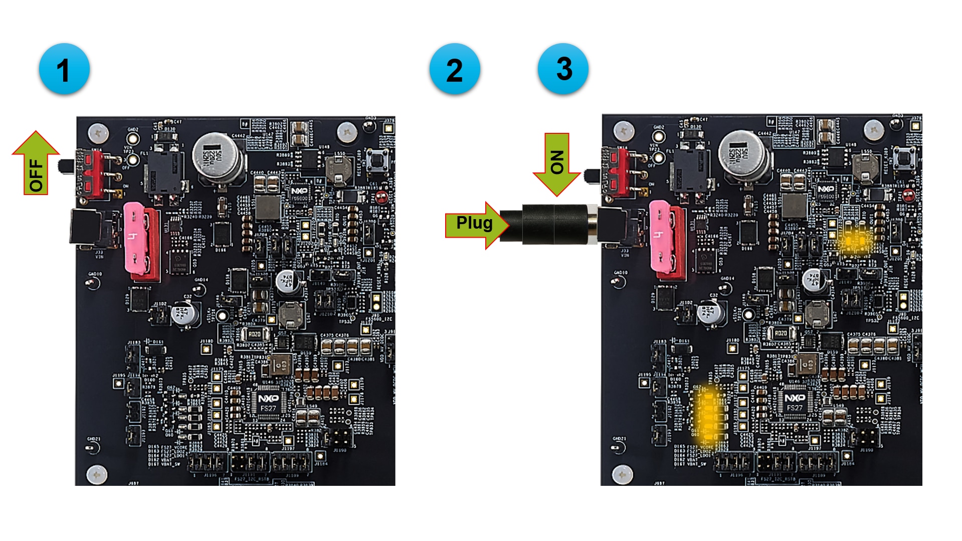
EVBに電源が投入されると、電圧レギュレータに隣接するオレンジ色のLEDが供給電圧の存在を示します。
3.3 デバッガの接続
S32K389EVB-Q437は、デフォルトで外部デバッガを使用するように設定されています。
MCUのプログラミングには、J1117 10ピン(0.05インチ)JTAGコネクタ、J38 20ピン(0.05インチ)JTAGコネクタ、またはP1 38ピンMictor ETMトレース・コネクタのいずれかを使用します。
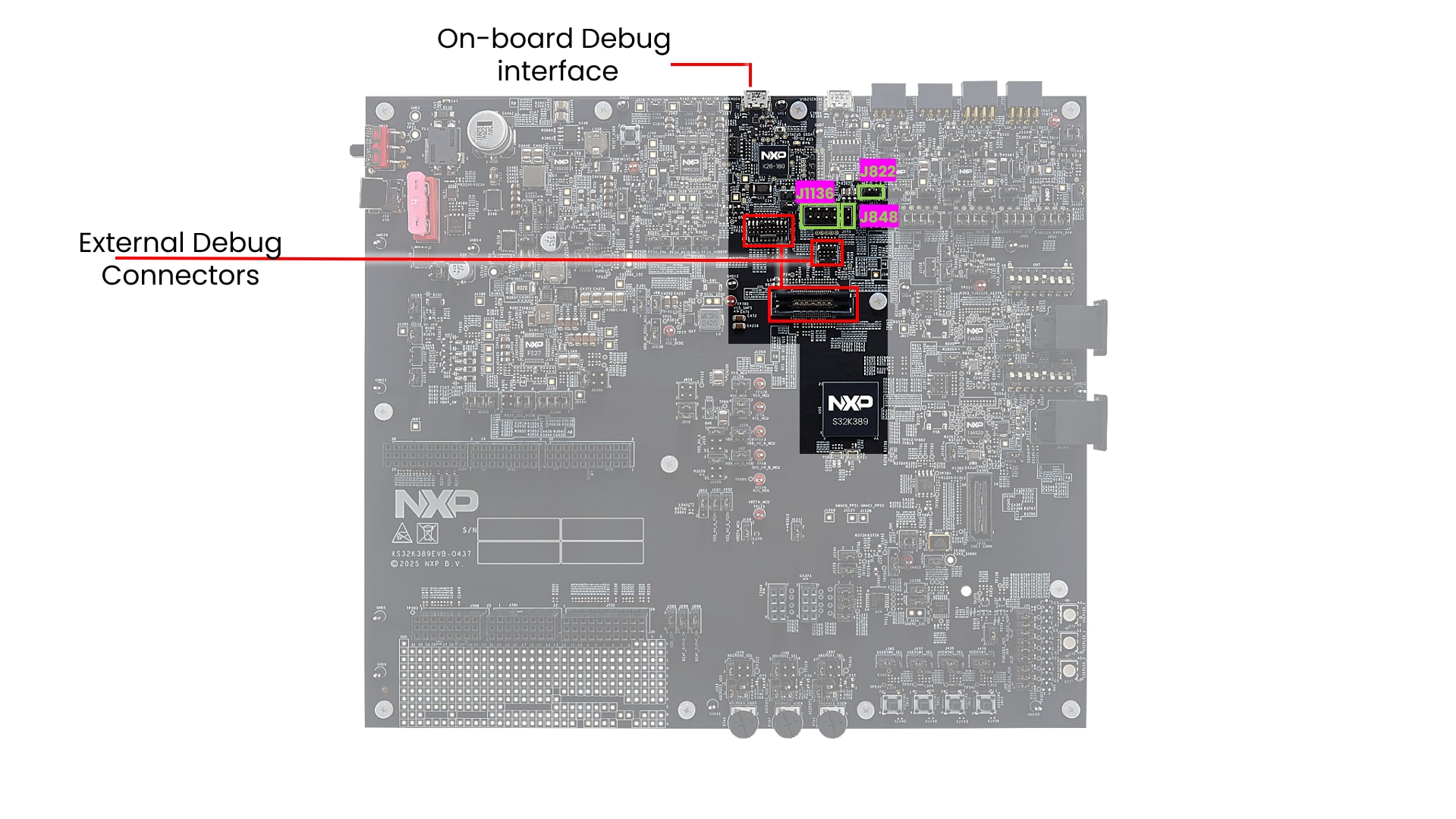
オンボードS32K3デバッグ・インターフェースとともに使用するには、ジャンパをJ822、J848、およびJ1136(1-2、3-4、5-6、7-8)に配置し、micro-USBケーブルをJ21コネクタに接続します。
4. アプリケーションの作成
S32K389EVB-Q437評価ボードを実際に使ってみましょう。
4.1 新規S32DSプロジェクトを最初から作成
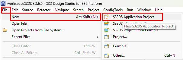
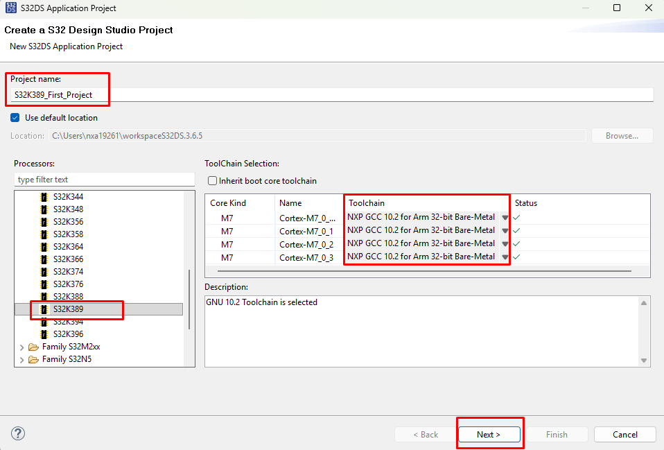
S32 Design Studio 3.6.5を起動します。メニューの[File(ファイル)]>[New(新規)]>[S32DS Application Project(S32DSアプリケーション・プロジェクト)]をクリックします
新しいプロジェクト名(スペースなし)を入力し、「S32K389」シリーズを選択します。
デフォルトのバージョン11.4ではなく、GCCバージョン10.2を選択します。インストールしたS32K3 RTDバージョン 7.0はGCCツールチェーン10.2用に作成されています。
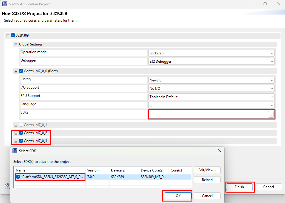
メイン・コア0用のSDK(S32K3 RTDバージョン7.0)を選択します。コア1は、ロックステップ構成におけるコア0のチェッカー・コアです。オプションとして、コア2およびコア3用のSDKを選択することもできます。
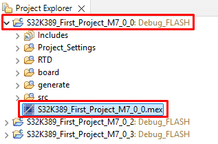
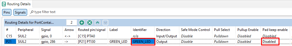
4.2 ピンの設定
1. プロジェクトのmexファイルをダブルクリックします
2. PTI30ピン(緑色LEDに接続済み)をGPIO出力として設定します
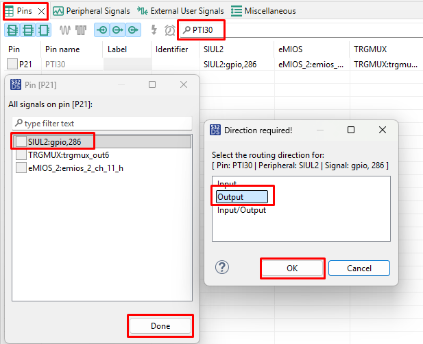
3. PTI30の識別子を定義します(スペースなし)。たとえば、「GREEN_LED」とします。[Pad keep enable(パッド・キープ・イネーブル)]オプションでは[Disable(ディセーブル)]を選択します。
4.3 ドライバの追加および構成ファイルの生成
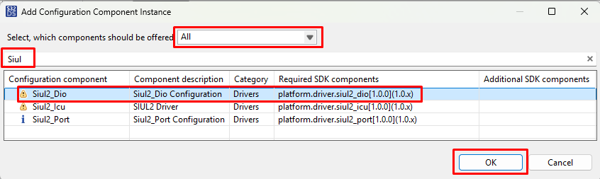
[Peripherals perspective(ペリフェラル画面)]に切り替えて、アプリケーションにSiul2_Dioドライバを追加します。

適切なプロジェクトを設定していることを確認し、[Update Code(コードの更新)]ボタンをクリックして設定ファイルを生成します。
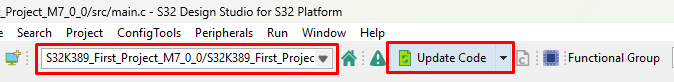
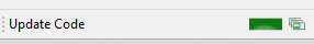
「Update Code(コードの更新)」が完了するまで待ちます。右下隅にステータス・バーが表示されます。
4.4 コードの編集
1. C/C++画面に戻ります。

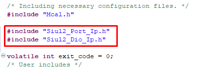
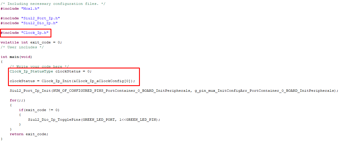
2. srcフォルダのmain.cファイルを編集し、「Port」および「Dio」ドライバを含めます。
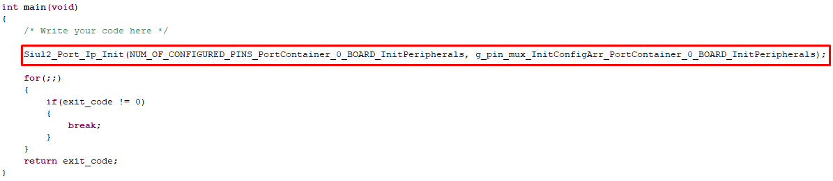
3. ピン初期化のコマンド・ラインを入力します。ボード・フォルダのSiul2_Port_Ip_Cfg.hファイルからパラメータをコピーすることができます。
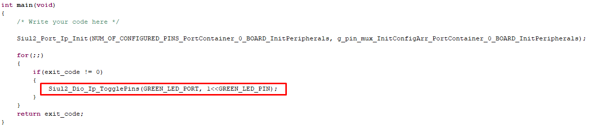
4. 最後に、GREEN_LEDピンを切り替えるためのコマンドも入力します
5. ビルドと実行
5.1 MCUへのソフトウェアのアップロード
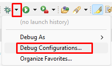
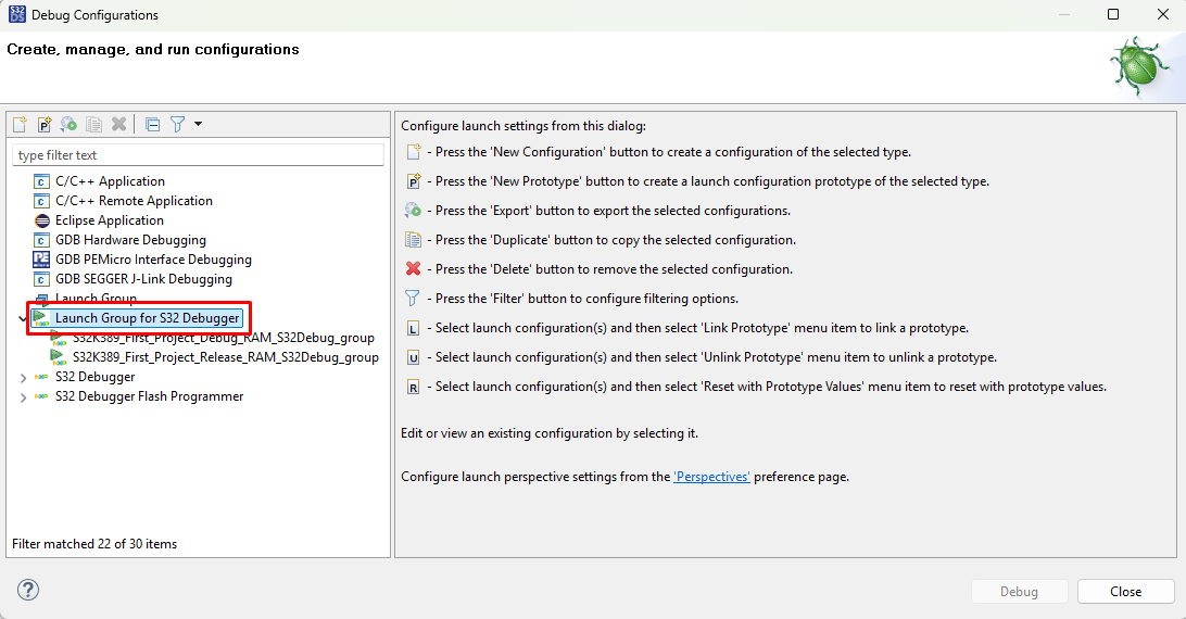
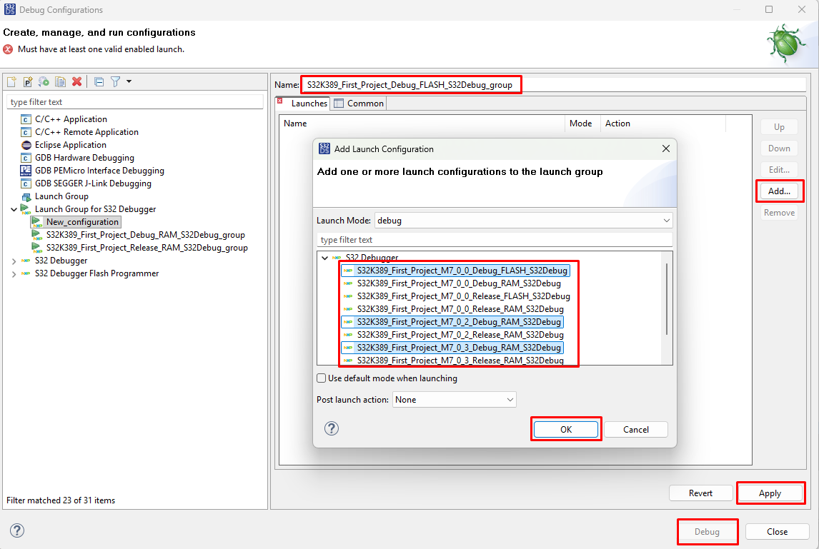
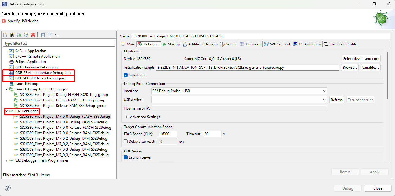
[Debug Configuration(デバッグ設定)]メニューを使用し、すべてのコアのソフトウェア・プロジェクトをビルドしてアップロードするための[Launch Group(起動グループ)]設定を選択します。
5.2 コードのデバッグ
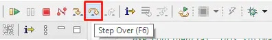
S32DSが[Debug(デバッグ)]画面に切り替わります。この画面でコードをステップ・オーバー (F6) することができます。
緑色LEDのオン/オフが無限ループで繰り返されます。
設計・リソース
チップに関するドキュメント
ソフトウェア
- 車載ソフトウェア・パッケージ・マネージャ
- S32K3標準ソフトウェア・パッケージ
- S32K3リファレンス・ソフトウェア・パッケージ
- S32 Design Studio IDE
- リアルタイム・ドライバ (RTD)
- S32K消費電力計算ツール (PET)
- モデルベース設計ツールボックス (MBDT)
- 構造コア・セルフテスト (SCST) ライブラリ
- FreeMASTERランタイム・デバッグ・ツール
- プラットフォーム間通信フレームワーク (IPCF)
- 車載用演算/モータ制御ライブラリ (AMMCLib)
- S32セーフティ・ソフトウェア・フレームワーク (SAF) およびセーフティ・ペリフェラル・ドライバ (SPD)