Getting Started with the RDGD31303PHG2EVB Evaluation Board
このドキュメントの内容
-
Out of the Box
-
Get To Know the Hardware
-
Plug It In
-
Build and Load
サインイン 進行状況を保存するには アカウントをお持ちでない方 アカウントを作成する。
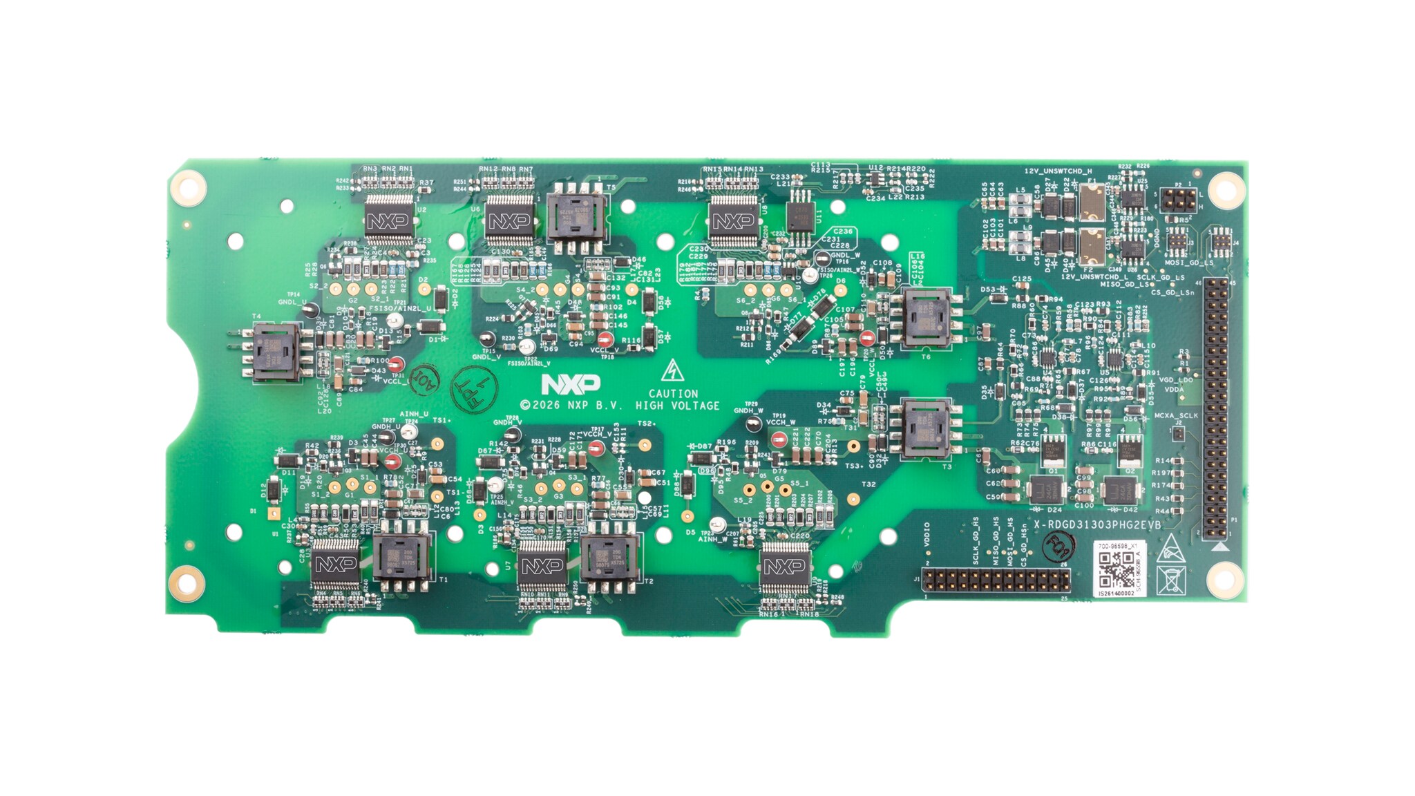
お客様の RDGD31303PHG2EVB - GD3130 Three-Phase Reference Design Kit
1. Out of the Box
NXP analog product development boards provide an easy-to-use platform to evaluate NXP products. The board supports a range of analog, mixed-signal and power solutions. They incorporate monolithic integrated circuits (ICs) and system-in-package (SiP) devices based on proven high-volume technologies. NXP products are designed to deliver longer battery life, smaller form factor, reduced component counts, lower costs and improved performance in powering state-of-the-art systems.
This guide walks you through the process of setting up and using the RDGD31303PHG2EVB evaluation board (EVB).
1.1 Kit Contents
The kit's contents include:
- Assembled and tested RDGD31303PHG2EVB (three-phase gate drive board populated with GD3130 5.0 V compatible gate driver devices) board in an antistatic bag
- Quick start guide
1.2 Additional Hardware
In addition to the kit contents, the following hardware is recommended when working with this reference board.
- KITGD31XXTREVM microcontroller (MCU) and translator kit for general board and gate-driver evaluation, or S32K396-HPWR-MC control board for three-phase inverter development Compatible silicon carbide (SiC) metal-oxide-semiconductor field-effect transistor (MOSFET) module (HybridPACK Drive G2)
- DC-link capacitor compatible with HybridPACK Drive G2 insulated-gate bipolar transistor (IGBT) SiC MOSFET module
- High voltage (HV) power supply with protection shields and hearing protection
- Current sensors for monitoring each phase current
- 12 V, 1.0 A DC power supply
- Four-channel oscilloscope with appropriate isolated probes
1.3 Minimum System Requirements
This reference design requires a Windows PC workstation. You will need a Windows PC workstation to evaluate the board. For best results, please ensure that your PC is equipped with the following: USB-enabled PC with Windows 11 installed.
1.4 Get Software
Installing software is necessary to work with this reference design. Software can be found at the RDGD31303PHG2EVB page.
- For use with the KITGD31XXTREVM: FlexGUI 2
- For three-phase inverter development with the S32K396-HPWR-MC control board:
- S32 Design Studio integrated development environment (IDE) for S32 Platform
- Automotive Math and Motor Control Library (AMMCLib)
- FreeMASTER 3.0 or later runtime debugging tool
- Motor Control Application Tuning (MCAT) tool
- Example code, GD3130 device-driver notes and GD31xx device-driver reference
2. Get To Know The Hardware
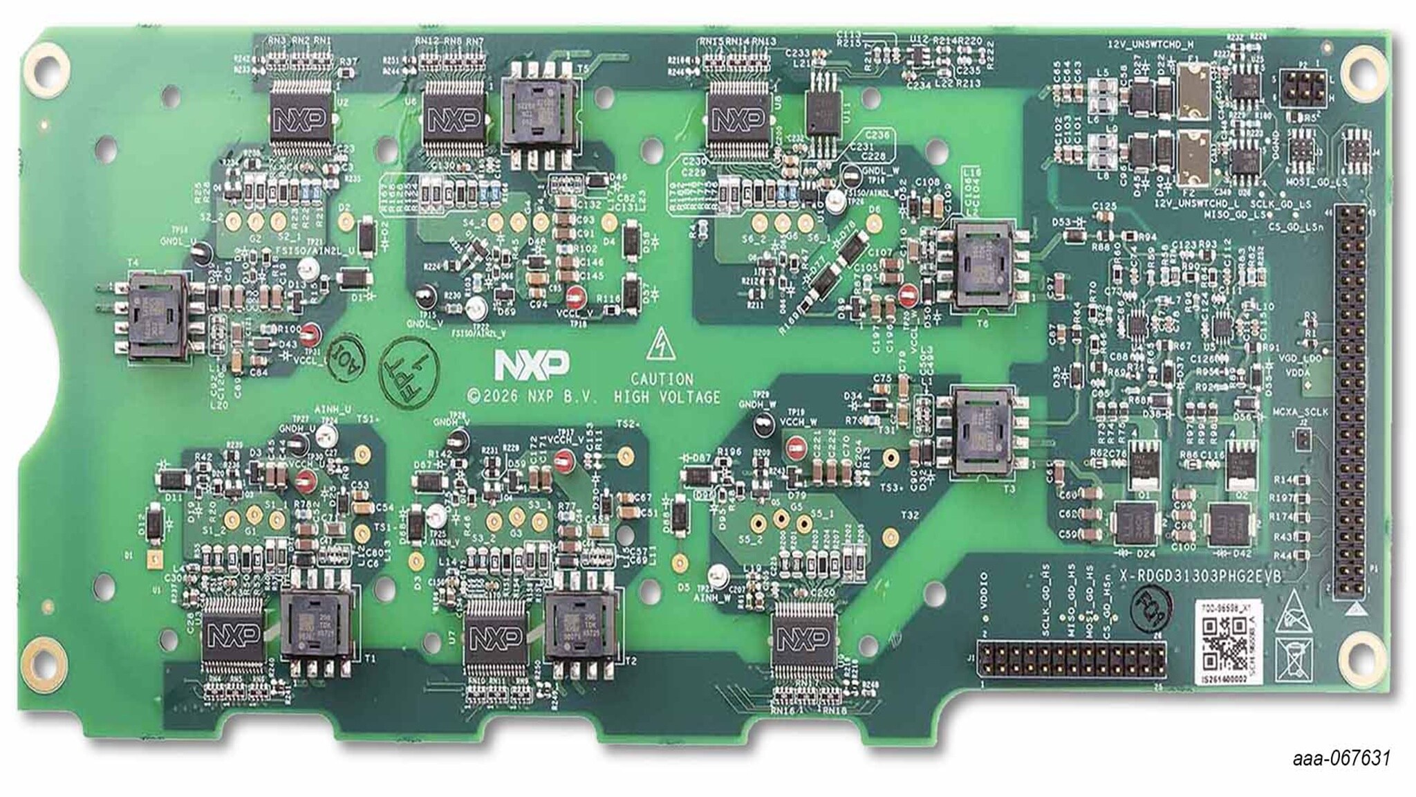
This section covers the features/components and provides a full description of the RDGD31303PHG2EVB. Refer to Figure 1 in this section to view how the board is oriented.
2.1 Board Features
Features of the RDGD31303PHG2EVB include:
- Capability to perform double pulse and short-circuit tests on any phase using jumper
J3andJ4jumper configurations and KITGD31XXTREVM with FlexGUI 2 software (some functions are limited to phase W); see phase schematics and FlexGUI 2 Pulse tab (Table 5 and Figure 14) - Evaluation board designed for and populated with GD3130 gate drivers and protection circuitry
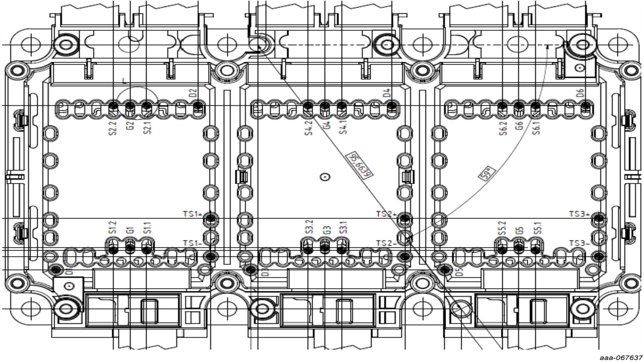
- Capability to connect to HybridPACK Drive G2 type SiC specific modules for full three-phase evaluation and development (see Figure 7 and Figure 8 for specific module pin placement)
- Daisy chain serial peripheral interface (SPI)communication (three high-side and three low-side gate drivers)
- Flyback positive supply voltage (VCC) power supply with isolated GND references and negative VEE supply
- Easy access to power, ground and signal test points
- 2 × 13-pin connector for using with KITGD31XXTREVM (MCU and translator kit)
- 2 × 23-pin connector for using with S32K396-HPWR-MC (MCU control board for inverters)
- Optional connection for DC bus voltage monitoring
2.2 Board Description
The RDGD31303PHG2EVB is a fully functional three-phase inverter evaluation board populated with six GD3130 gate drivers with fault management and supporting circuitry. This board supports SPI daisy chain communication for programming and communication with three high-side gate drivers and three low-side gate drivers independently. The board can be used with KITGD31XXTREVM MCXA153 small evaluation MCU board kit, or can be used with S32K396-HPWR-MC MCU for full inverter platforms development.
This board has low-voltage isolation and high-voltage isolation with gate drive integrated galvanic signal isolation. Additional supporting features on the board include desaturation-based short-circuit detection, IGBT/SiC temperature sensing and DC-link voltage monitoring. See GD3130 data sheet for all additional gate drive features.
2.3 Board Components
Below are full descriptions of the RDGD31303PHG2EVB board components. Refer to the images and tables provided in this section for a comprehensive overview of the board and how the components work.
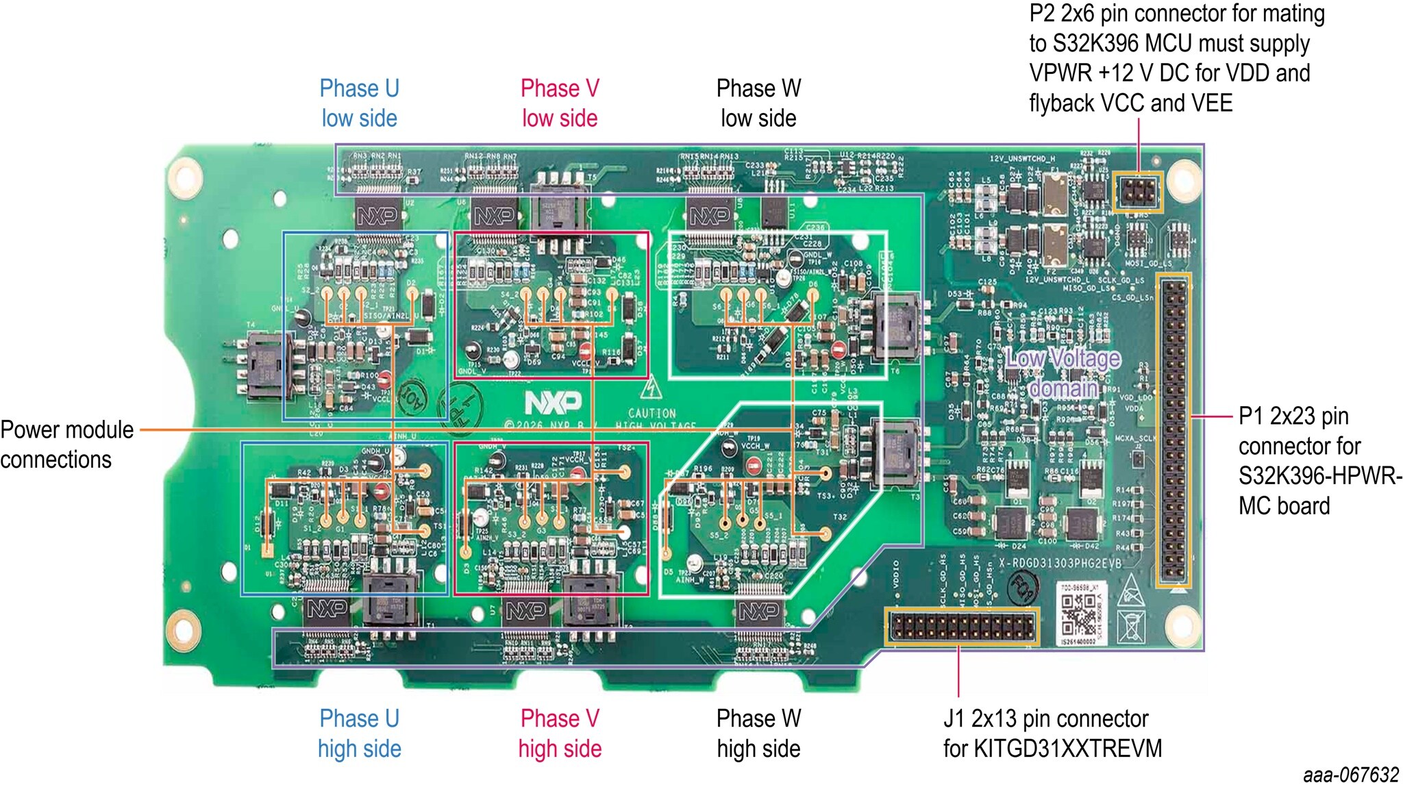
2.4 Voltage Domains, GD3130 Pinout And Logic Connection Headers
Low-voltage domain is an externally supplied 12 V DC (VPWR) primary supply for non-isolated circuits, typically supplied by a vehicle battery. A 5 V regulator supplies VDD to GD3130 gate drive devices derived from 1VPWR. The low-voltage domain includes the interface between the MCU and GD3130 control registers and logic control.
Low-side driver and high-side driver domains are isolated high-voltage driver control domains for SiC MOSFET or IGBT single phase connections and control circuits. Mill-Max pins (part number 0405-0-15-15-34-27-04-0) can be installed on the bottom of the board to connect easily to a compatible three-phase SiC MOSFET or IGBT module.
2.5 Gd3130 Pinout And MCU Interfaces And Power Domains
See GD3130 advanced IGBT/SiC gate driver data sheet for specific information about pinout, pin descriptions, specifications and operating modes. The P2 VPWR terminal supplies DC power to the nonisolated die and related circuitry in the low-voltage domain. The input is typically supplied by vehicle battery +12 V DC.
The 2 × 23-pin P1 connector interfaces with the S32K396-HPWR-MC control board or another compatible MCU board. . An MCU is needed for SPI communication and control of advanced IGBT/SiC gate drive devices (GD3130).
The KITGD31XXTREVM (not included) can be connect to this board at J1 header pin interface. FlexGUI 2 provides SPI access to all six gate drivers.
Note: Double-pulse and short-circuit tests can be conducted on any phase using FlexGUI 2; see Figure 14 and Table 5.
The following diagram and tables detail the board's connections.
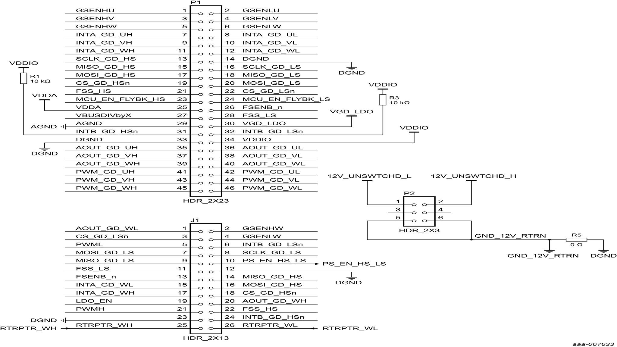
Figure 3. Gate Driver Board Interface Connections Diagram
| Pin | Name | Function |
|---|---|---|
| 1 | GSENHU | Gate-strength enable high-side (HS) phase U |
| 2 | GSENLU | Gate-strengthenable low-side (LS) phase U |
| 3 | GSENHV | Gate-strength enable HS phase V |
| 4 | GSENLV | Gate-strength enable LS phase V |
| 5 | GSENHW | Gate-strength enable HS phase W |
| 6 | GSENLW | Gate-strength enable LS phase W |
| 7 | INTA_GD_UH | Fault indicator HS phase U |
| 8 | INTA_GD_UL | Fault indicator LS phase U |
| 9 | INTA_GD_VH | Fault indicator HS phase V |
| 10 | INTA_GD_VL | Fault indicator LS phase V |
| 11 | INTA_GD_WH | Fault indicator HS phase W |
| 12 | INTA_GD_WL | Fault indicator LS phase W |
| 13 | SCLK_GD_HS | SPI HS clock |
| 14 | DGND | Low-voltage domain digital ground |
| 15 | MISO_GD_HS | SPI HS controller input target output |
| 16 | SCLK_GD_LS | SPI LS clock |
| 17 | MOSI_GD_HS | SPI HS controller output target input |
| 18 | MISO_GD_LS | SPI LS controller input target output |
| 19 | CS_GD_HS | SPI HS chip select |
| 20 | MOSI_GD_LS | SPI LS controller output target input |
| 21 | FSS_HS | Fail-safe-state HS |
| 22 | CS_GD_LSn | SPI LS chip select |
| 23 | MCU_EN_FLYBK_HS | Flyback enable for HS |
| 24 | MCU_EN_FLYBK_LS | Flyback enable for LS |
| 25 | VDDA | Analog supply for 5 V DC measurement |
| 26 | FSENB_n | Active-low fail-safe-state for HS and LS |
| 27 | VBUSDIVbyX | Bus voltage measurement |
| 28 | FSS_LS | Fail-safe-state LS |
| 29 | AGND | Analog ground |
| 30 | VGD_LDO | Power supply for low side logic |
| 31 | INTB_GD_HSn | HS fault indicator |
| 32 | INTB_GD_LSn | LS fault indicator |
| 33 | DGND | Digital ground |
| 34 | VDDIO | Power supply for HS logic |
| 35 | AOUT_GD_UH | Analog output (AOUT) pin output HS phase U |
| 36 | AOUT_GD_UL | AOUT pin output for LS phase U |
| 37 | AOUT_GD_VH | AOUT pin output for HS phase V |
| 38 | AOUT_GD_VL | AOUT pin output for LS phase V |
| 39 | AOUT_GD_WH | AOUT pin output for HS phase W |
| 40 | AOUT_GD_WL | AOUT pin output for LS phase W |
| 41 | PWM_GD_UH | Pulse width modulation (PWM) input HS phase U |
| 42 | PWM_GD_UL | PWM input for LS phase U |
| 43 | PWM_GD_VH | PWM input for HS phase V |
| 44 | PWM_GD_VL | PWM input for LS phase V |
| 45 | PWM_GD_WH | PWM input for HS phase W |
| 46 | PWM_GD_WL | PWM input for LS phase W |
| Pin | Name | Function |
|---|---|---|
| 1 | AOUT_GD_WL | AOUT pin output for LS phase W |
| 2 | GSENHW | Gate-strength enable for HS phase W |
| 3 | CS_GD_LSn | Chip select low side |
| 4 | GSENLW | Gate-strength enable for HS phase W |
| 5 | PWML | PWM input for the LS gate drivers; configurable for any phase through J3 |
| 6 | INTB_GD_LSn | Fault indicator for LS |
| 7 | MOSI_GD_LS | SPI controller output and target input for LS |
| 8 | SCLK_GD_LS | SPI clock for LS |
| 9 | MISO_GD_LS | SPI controller input and target output for LS |
| 10 | PS_EN_HS_LS | Flyback enable for HS and LS |
| 11 | FSS_LS | Fail-safe-state LS |
| 12 | DGND | Digital ground |
| 13 | FSENB_n | Active-low fail-safe-state enable for HS and LS |
| 14 | MISO_GD_HS | SPI controller input and target output for HS |
| 15 | INTA_GD_WL | Fault indicator for LS phase W |
| 16 | MOSI_GD_HS | SPI controller input and target output for HS |
| 17 | INTA_GD_WH | Fault indicator for HS phase W |
| 18 | CS_GD_HSn | Chip select for high side |
| 19 | LDO_EN | 5 V for voltage regulators supplying VDDIO and VGDLDO |
| 20 | AOUT_GD_WH | AOUT pin output HS phase W |
| 21 | PWMH | PWM input for HS can jumper to any phase via J3 |
| 22 | FSS_HS | Fail-safe-state input for high side |
| 23 | DGND | Digital ground |
| 24 | INTB_GD_HSn | Fault indicator for high side |
| 25 | RTRPTR_WH | Real-time report output for HS phase W |
| 26 | RTRPTR_WL | Real-time report output for LS phase W |
| Pin | Name | Function |
|---|---|---|
| 1 | 12V_UNSWTCHD_L | 12 V DC input for the LS gate drivers; can be connected to the HS 12 V input |
| 2 | 12V_UNSWTCHD_H | 12 V DC input for the HS gate drivers; can be connected to the LS 12 V input |
| 3 | n.c. | Fault reporting and real-time monitoring for GD3162 LS phase W |
| 4 | n.c. | Fail-safe-state enable bar |
| 5 | GND_12V_RTRN | Fail-safe-state LS |
| 6 | GND_12V_RTRN | Fail-safe-state HS |
2.6 Test Points
Figure 4 below shows the location of various test points with each clearly marked on the board. Table 4 (immediately below Figure 4) describes each labeled test point.
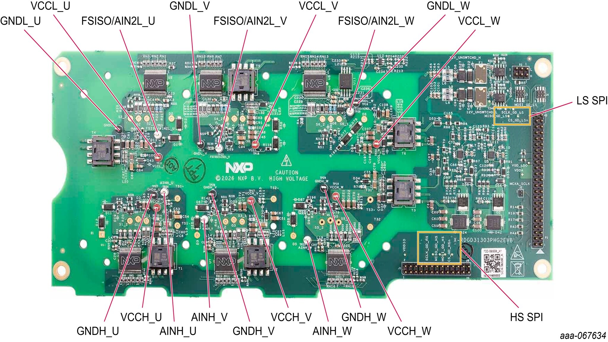
| Test Point Name | Function |
|---|---|
| GNDL_U | Isolated ground for LS phase U |
| VCCL_U | Isolated VCC for LS phase U |
| FSISO/AIN2L_U | Fail-safe isolation (FSISO) or AIN2 input for LS phase U (selectable using FSISO_EN) |
| GNDH_U | Isolated ground for HS phase U |
| VCCH_U | Isolated VCC for HS phase U |
| AINH_U | Analog input (AIN) for HS phase U |
| GNDL_V | Isolated ground for LS phase V |
| FSISO/AIN2L_V | FSISO or AIN2 input for LS phase V (selectable via FSISO_EN) |
| VCCL_V | Isolated VCC for LS phase V |
| AINH_V | AIN for HS phase V |
| GNDH_V | Isolated ground for HS phase V |
| VCCH_V | Isolated VCC for HS phase V |
| FSISO/AIN2L_W | FSISO or AIN2 input LS phase W (selectable via FSISO_EN) |
| GNDL_W | Isolated ground LS phase W |
| VCCL_W | Isolated VCC LS phase W |
| AINH_W | AIN analog input HS phase W |
| GNDH_W | Isolated ground HS phase W |
| VCCH_W | Isolated VCC HS phase W |
| LS SPI | PCB test points for LS SPI (low-voltage domain) |
| HS SPI | PCB test points for HS SPI (low-voltage domain) |
2.7 Connectors and Jumpers
Figure 5 below identifies the connectors and jumpers. Table 5 (immediately below Figure 5) describes each labeled jumper.
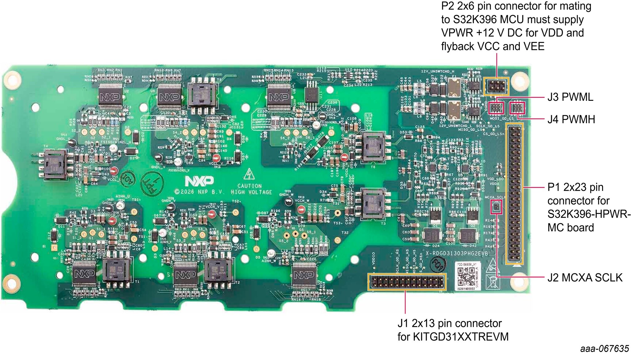
| Name | Description |
|---|---|
| P2 (For use with KITGD31XXTREVM and S32K396-HPWR-MC) |
External 12 V DC power-supply connection compatible with the S32K396-HPWR-MC control board. Connect 12 V DC to the RDGD31303PHG2EVB as follows:
|
| P1 (For use with S32K396-HPWR-MC) | 46-pinheader connector compatible with S32K396-HPWR-MC (MCU control board) |
J1 (For use with KITGD31XXTREVM) |
26-pinheader connector compatible with KITGD31XXTREVM (MCU and translator kit); enables ability to access all gate drivers high side and low side via (x3 - 2 channel) daisy chain* |
J2 (For use with KITGD31XXTREVM) |
Connects the high-side and low-side serial peripheral interface (SPI) clock signals to the MCXA153 SPI clock. Use only with the KITGD31XXTREVM |
J3 (For use with KITGD31XXTREVM) |
Selects the LS phase that receives the PWML signal when using the KITGD31XXTREVM for double-pulse and short-circuit testing:
|
J4 (For use with KITGD31XXTREVM) |
Selects the high-side phase that receives the PWMH signal when using the KITGD31XXTREVM for double-pulse and short-circuit testing:
|
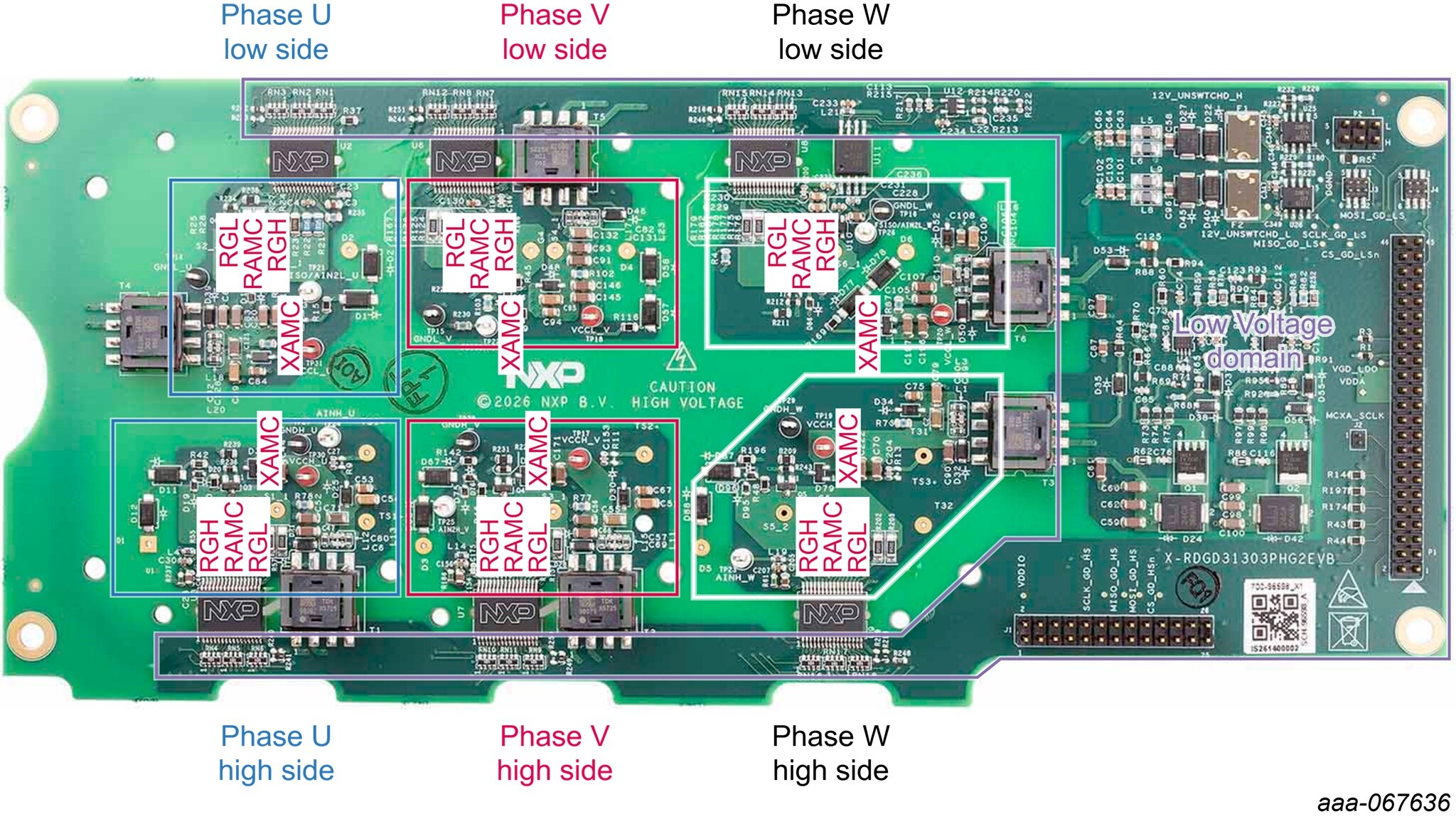
2.8 Gate Drive Resistors
The following list describes each gate-driver resistor and its function:
- RGH_1: gate high resistor in series with the GH_1 pin at the output of the GD3130 high-side driver and IGBT/ SiC gate that controls the strong turn-on current for IGBT/SiC gate
- RGH_2: gate high resistor in series with the GH_2 pin at the output of the GD3130 high-side driver and IGBT/ SiC gate that controls the weak turn-on current for IGBT/SiC gate
- RGL_1: gate low resistor in series with the GL_1 pin at the output of the GD3130 low-side driver and IGBT/ SiC gate that controls the strong turn-off current for IGBT/SiC gate
- RGL_2: gate low resistor in series with the GL_2 pin at the output of the GD3130 low-side driver and IGBT/ SiC gate that controls the weak turn-off current for IGBT/SiC gate
- RAMC: - series resistor between IGBT/SiC gate and active Miller clamp (AMC) input pin of the GD3130 high‑side/low-side driver for gate sensing and active Miller clamping
- XAMC: external AMC field effect transistor (FET) for higher AMC current controlled by GD3130 predriver output logic
The following figures and tables detail the gate drive resistors and pin connections.
2.9 SIC Module Pin Connections
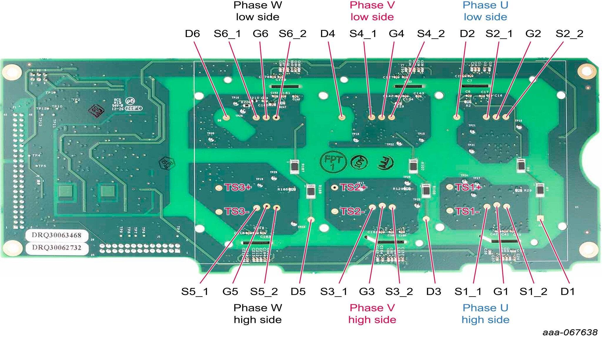
| Connection name | Pin description |
|---|---|
| D6 | Drain for LS phase W |
| S6_1 | Source 1 for LS phase W |
| G6 | Gate for LS phase W |
| S6_2 | Source 2 for LS phase W |
| D4 | Drain LS for phase V |
| S4_1 | Source 1 for LS phase V |
| G4 | Gate for LS phase V |
| S4_2 | Source for LS phase V |
| D2 | Drain for LS phase U |
| S2_1 | Source 1 for LS phase U |
| G2 | Gate for LS phase U |
| S2_2 | Source 2 for LS phase U |
| S5_1 | Source 1 for HS phase W |
| G5 | Gate for HS phase W |
| S5_2 | Source 2 for HS phase W |
| D5 | Drain for HS phase W |
| S3_1 | Source 1 for HS phase V |
| G3 | Gate for HS phase V |
| S3_2 | Source 2 for HS phase V |
| D3 | Drain for HS phase V |
| S1_1 | Source 1 for HS phase U |
| G1 | Gate for HS phase U |
| S1_2 | Source 2 for HS phase U |
| D1 | Drain for HS phase U |
| TS3+ | Temperature-sensing (TS) diode anode phase W |
| TS3- | TS diode cathode phase W |
| TS2+ | TS diode anode phase V |
| TS2- | TS diode cathode phase V |
| TS1+ | TS diode anode phase U |
| TS1- | TS diode cathode phase U |
3. Plug It In
Download FlexGUI 2 for Windows from the FlexGUI software page. The FlexGUI 2 package includes the firmware for the FRDM-MCXA153 microcontroller unit (MCU) board
It is recommended that you install FlexGUI 2 even if you plan to control the board using another software or PWM method. With FlexGUI 2, you can verify communication and troubleshoot the board configuration.
3.1 Installing Flexgui 2 On Your PC
The latest version of FlexGUI 2 supports all GD3100, GD3160, GD3162 and GD313x. It is designed to run on any Windows 11 based operating system. To install the software, follow these steps:
- Go to the FlexGUI software page and click DOWNLOADS
- Select FlexGUI 2 for GD3100/GD3160/ GD3162 Advanced Gate Driver Evaluation Software
- Click Download downloads the flexgui-app zip file to your download folder
- Extract or unzip the file and go to the GUI folder to install on your PC
- Run “
NXP_GD31xx_GUI_public-x.x.x.msi” - Follow the installation steps
- When the installation is complete, a FlexGUI 2 shortcut icon will appear on the desktop as
NXP_GD31xx_GUI_public
Note: The installer replaces any previous FlexGUI installation with the current version containing the GD31xx drivers. However, existing spi configuration files will remain intact.
3.2 Configuring The Frdm-Mcxa153 Microcode
Refer to Figure 9 and the instructions below to configure the microcode for the FRDM-MCXA153.
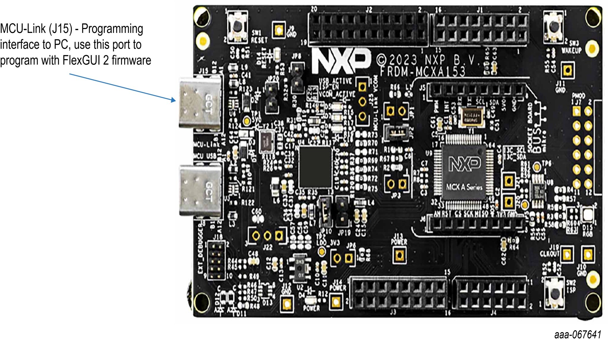
To program the latest firmware on the FRDM-MCXA153 board, download and install LinkServer for Windows from the LinkServer page.
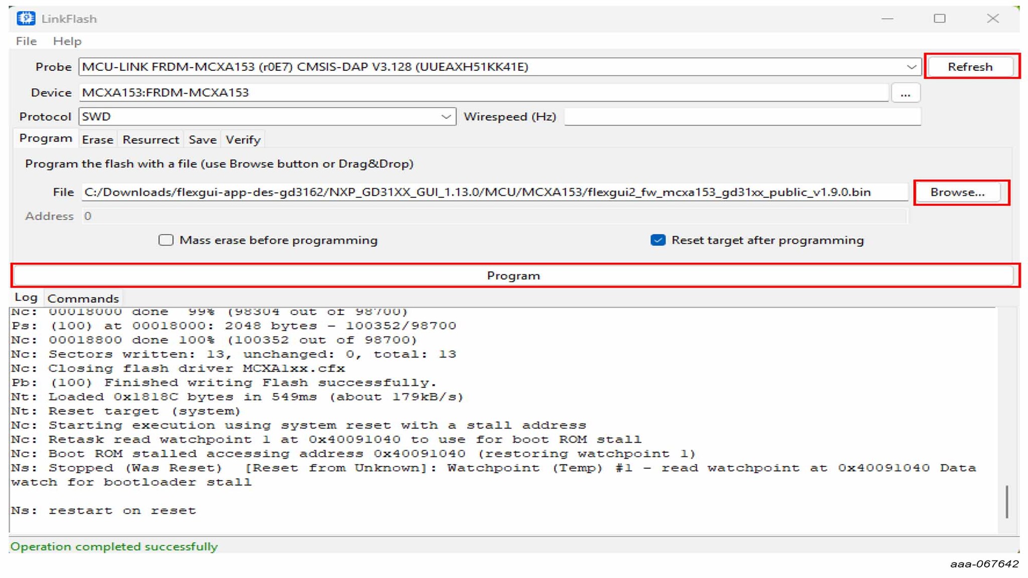
- Install LinkServer. The LinkFlash shortcut appears on the desktop when installation is complete
- Open LinkFlash
- Connect a USB Type-C cable between the Windows PC and the MCU-Link USB Type-C port,
J15, on the FRDM-MCXA153 board - In LinkFlash, select Refresh
- Verify that MCU-LINK FRDM-MCXA153 appears in the Probe and Device field, as shown in Figure 10
- From the File menu, browse to the MCU folder in the extracted FlexGUI 2 package
- Open the MCXA153 folder and select
flexgui2_fw_mcxa153_gd31xx_public_vx.x.x.bin - Set Start address to 0
- Select Program
- When programming is complete, “Operation completed successfully” will appear at the bottom of the LinkFlash window, as shown in Figure 10
4. Build and Load
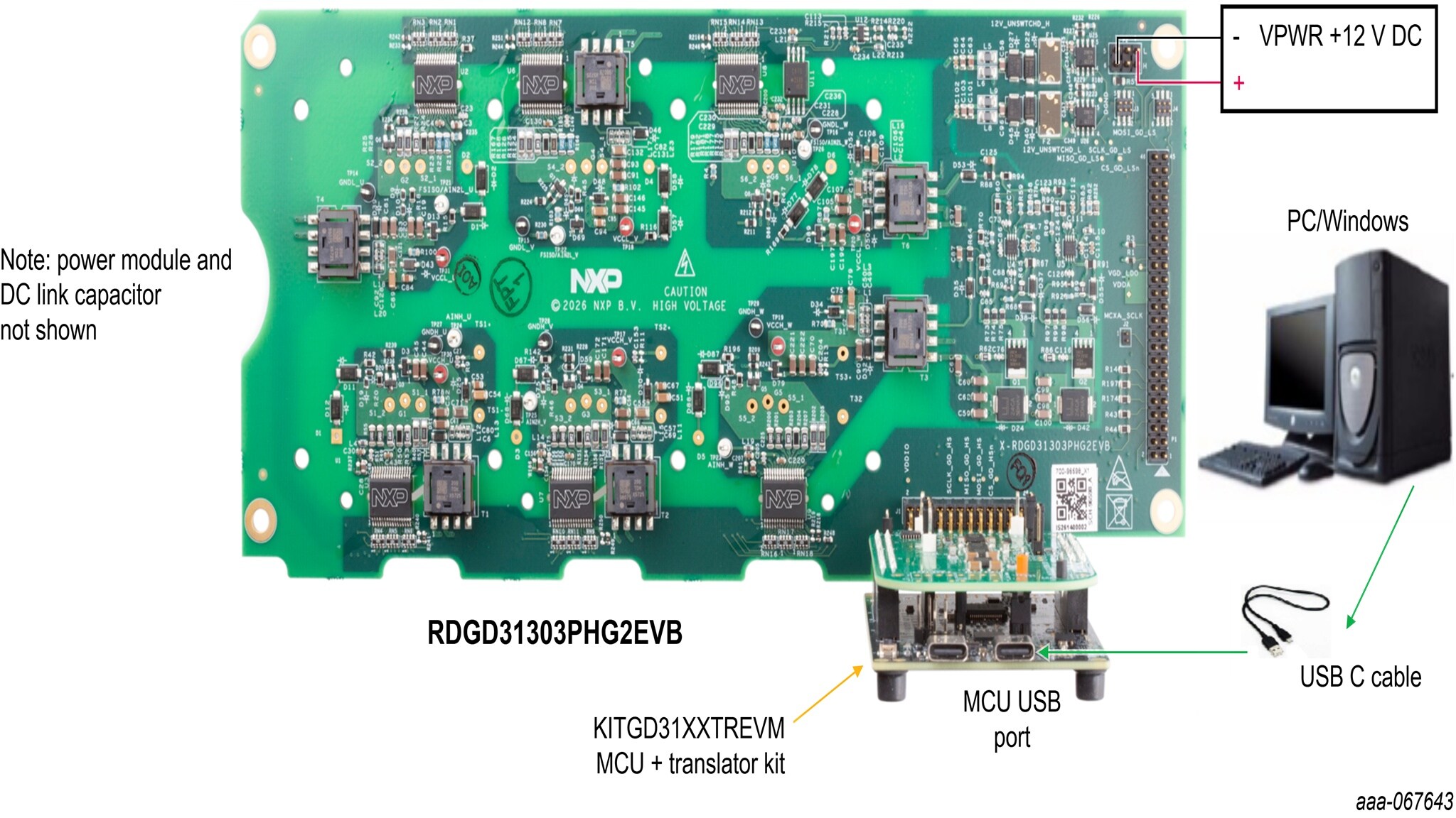
Connect the RDGD31303PHG2EVB to a compatible HybridPACK Drive G2 silicon carbide metal-oxide-semiconductor field-effect transistor (SiC MOSFET) module and DC-link capacitor, as shown in Figure 11. You can then use FlexGUI 2 on a Windows PC to perform double-pulse and short-circuit testing.
The following equipment is recommended for the test configuration:
- Rogowski coil high-current probe
- High-voltage differential voltage probe for measuring drain-to-source voltage
- High-sample-rate digital oscilloscope with probes
- DC-link capacitor compatible with HybridPACK Drive G2 power module
- HybridPACK Drive G2 power module
- Windows-based PC
- High-voltage DC power supply for DC-link voltage
- Low-voltage DC power supply for supply voltage (VSUP)
- +12 V DC gate-driver board's low-voltage domain
- Digital voltmeter for monitoring high-voltage DC-link supply
- Load coil for double-pulse testing
Connect the cables and power supply as follows:
- Connect the KITGD31XXTREVM (MCU + translator) to
J1of RDGD31303PHG2EVB - Connect a USB Type-C cable between the MCU-Link USB Type-C port on the FRDM-MCXA153 MCU and a USB port on the Windows PC
- On the RDGD31303PHG2EVB, connect the positive output of the 12 V DC power supply to the VSUP terminals at P2 pins 1 and 2
- Connect the power-supply ground to the GND terminals at P2 pins 5 and 6
4.1 Build and Load
Connect the RDGD31303PHG2EVB to a compatible HybridPACK Drive G2 silicon carbide metal-oxide-semiconductor field-effect transistor (SiC MOSFET) module and DC-link capacitor, as shown in Figure 11. You can then use FlexGUI 2 on a Windows PC to perform double-pulse and short-circuit testing.
The following equipment is recommended for the test configuration:
- Rogowski coil high-current probe
- High-voltage differential voltage probe for measuring drain-to-source voltage
- High-sample-rate digital oscilloscope with probes
- DC-link capacitor compatible with HybridPACK Drive G2 power module
- HybridPACK Drive G2 power module
- Windows-based PC
- High-voltage DC power supply for DC-link voltage
- Low-voltage DC power supply for supply voltage (VSUP)
- +12 V DC gate-driver board's low-voltage domain
- Digital voltmeter for monitoring high-voltage DC-link supply
- Load coil for double-pulse testing
Connect the cables and power supply as follows:
- Connect the KITGD31XXTREVM (MCU + translator) to
J1of RDGD31303PHG2EVB - Connect a USB Type-C cable between the MCU-Link USB Type-C port on the FRDM-MCXA153 MCU and a USB port on the Windows PC
- On the RDGD31303PHG2EVB, connect the positive output of the 12 V DC power supply to the VSUP terminals at P2 pins 1 and 2
- Connect the power-supply ground to the GND terminals at P2 pins 5 and 6
Design Resources
The resources listed below have been curated to support you through the evaluation and development process.
Board Information
Additional References
For additional support, please refer to the following resources:
- GD3130: Product information on advanced single‑channel gate driver for IGBT/SiC
- EV-INVERTERGEN3: Three-phase inverter platform using S32K396-HPWR-MC board and GD3162 power board
- MPC5775B-EVB and MPC5775E-EVB: Low-cost development board for battery management and inverter