Getting Started with the KITFS85SKTEVM
このドキュメントの内容
-
Get Started
-
Know the Board
-
Configure Hardware
-
Install Software
サインイン 進行状況を保存するには アカウントをお持ちでない方 アカウントを作成する。
お客様の FS84/FS85/FS66 Safety SBC Programming Boards
1. Get Started
The NXP analog product development boards provide an easy-to-use platform for evaluating NXP products. The boards support a range of analog, mixed-signal, and power solutions. They incorporate monolithic integrated circuits and system-in-package devices that use proven high-volume technology. NXP products offer longer battery life, a smaller form factor, reduced component counts, lower cost and improved performance in powering state-of-the-art systems.
This page will guide you through learning about how to set up the KITFS85SKTEVM board.
1.1 Kit contents/packing list
Working with the KITFS85SKTEVM requires the kit contents, additional hardware and a Windows PC workstation with installed software.
1.2 Kit contents
- Assembled and tested evaluation board in an anti-static bag
- 3.0 ft USB-STD A to USB-B-mini cable
- Two connectors, terminal block plug, 2 pos., str. 3.81 mm
- Three connectors, terminal block plug, 3 pos., str. 3.81 mm
- Jumpers mounted on board
1.3 Additional hardware
In addition to the kit contents, the following hardware is necessary or beneficial when working with this kit.
- Power supply with a range of 8.0 V to 60 V and a current limit set initially to 1.0 A (maximum current consumption can be up to 6.0 A)
1.4 Windows PC workstation
This evaluation board requires a Windows PC workstation. Meeting these minimum specifications should produce great results when working with this evaluation board.
- USB-enabled computer with Windows 7 or Windows 10
1.5 Software
Installing software is necessary to work with this evaluation board. All listed software is available on the evaluation board's information page at KITFS85SKTEVM.
- Last FlexGUI available (PC host software to control the kit)
- Java JRE (Java SE Runtime Environment)
To generate Device OTP programming and emulation you will need the following:
- FS85_FS84_OTP_Configuration.xls spreadsheet
1.6 User manual
Refer to UM11183 for full evaluation board functionality.
2. Know the Board
2.1 Board features
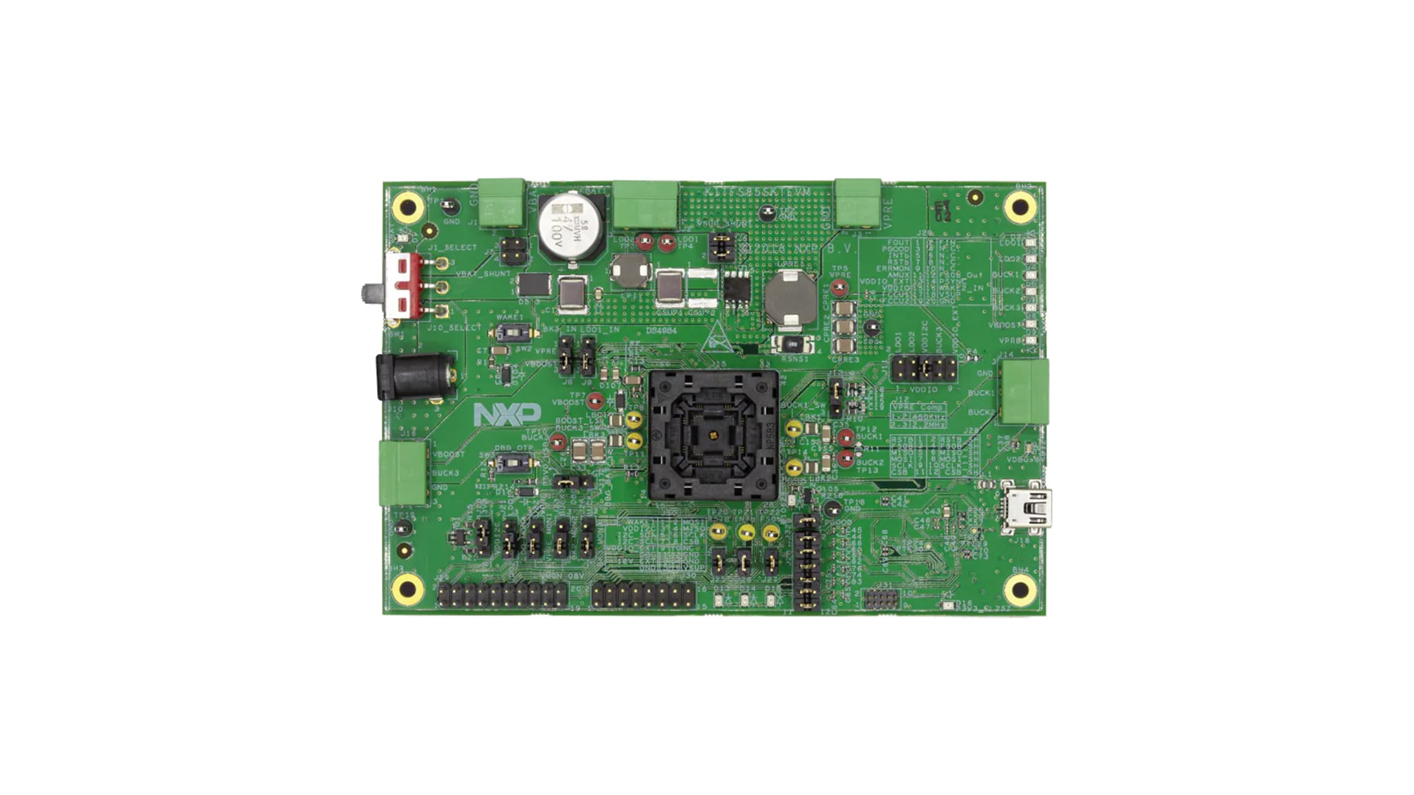
The KITFS85KTEVM provides flexibility to play with all the features of the device and make measurements on the main part of the application. The KL25Z MCU installed on the board, combined with the FlexGUI software allows access to the registers in read and write mode. All regulators are accessible through connectors. Nonuser signals, like DC/ DC switcher nodes are mapped on test points. Digital signals (SPI, I²C, RSTb, etc.) are accessible through connectors. Wake1 pin has a switch to control (Ignition) them. A VBAT switch is available to power On or Off the device.
The main purpose of this kit is to burn the OTP configuration.
The KITFS85KTMEVM is a hardware evaluation tool that allows OTP burning. Due to the socket, the FS84/FS85 part can be configured without the need to solder it. Devices can be programmed three times.
2.2 KITFS85SKTEVM evaluation board features
- VBAT power supply connectors (Jack and Phoenix)
- VPRE output capability up to 1.0 A (socket limit)
- VBUCK1/2 in Standalone (default) or Multiphase mode
- VBUCK3
- VBOOST 5.0 V or 5.74 V
- LDO1 and LDO2, from 1.1 V to 5.0 V
- Ignition key switch
- FS0B external safety pin
- Embedded USB connection for easy connection to software GUI (access to SPI/I²C bus, IOs, RSTB, FS0B, INTB, Debug, MUX_OUT, regulator)
- LEDs that indicate signal or regulator status
- Support OTP fuse capabilities
- USB connection for register access, OTP emulation and programming
- Voltage monitoring jumper setting
*Integrated FRDM-KL25Z as a communication link between the EVB and a PC
| Device | Description | Features |
|---|---|---|
| FS8500 | Safety System Basis Chip for S32 Microcontrollers |
|
| FS8400 | Safety System Basis Chip for S32 Microcontrollers |
|
2.3 Board Descriptions
The KITFS85KTMEVM is a hardware evaluation tool that allows OTP burning. Due to the socket, the FS84/FS85 part can be configured without the need to solder it. Devices can be programmed three times. An Emulation mode is possible to test as many configurations as needed. An external LDO provides VDDI²C voltage with a choice of 1.8 V or 3.3 V (default). VDDIO is assigned by default to VDDI²C. From USB voltaage, an external DC/DC generates the OTP programming voltage (8.0 V) without any need for an external power supply.
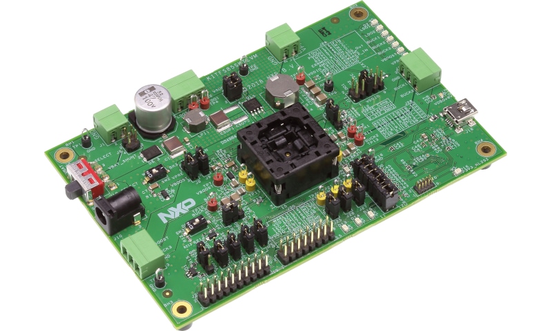
2.4 Board Image
2.5 Additional board support
Board block diagram, jumpers, test points, connectors, switches, OTP device configurations and additional board descriptions / images are available in the User Guide. Refer to UM11183.
3. Configure Hardware
3.1 Configure the hardware
This section summarizes the overall setup. Detail description is provided in the user guide.
Suggested equipment's needed for test:
- 8.0 V to 40 V power supply
- Computer
- Mini USB type A Cable
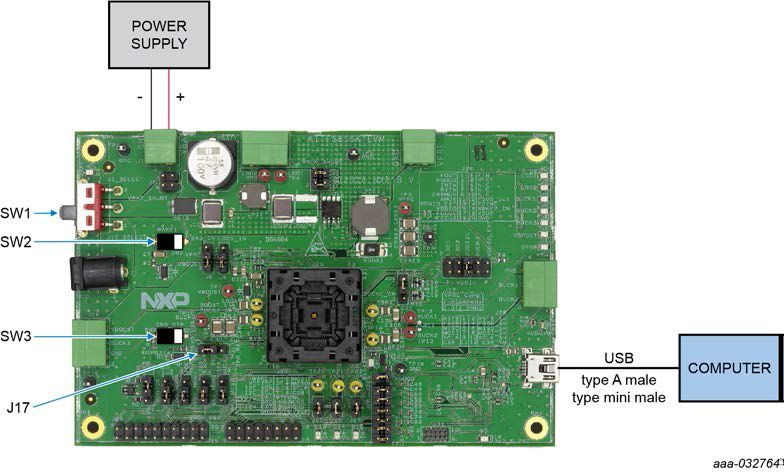
3.2 Configuration image
3.3 Device Considerations
It is recommended to learn about OTP before operating with the device. The device has a high level of flexibility due to parameter configuration available in the OTP. This impacts the functionality of the device. It is key to understand how OTP parameters can be programmed, the interaction with mirror registers and the FS85 SoC. The OTP related operations can be performed either in Emulation mode, where the product uses a given configuration if the power supply is not switched Off or from OTP fuse content that is valid even after a power down/power up sequence.
3.4 Setting up the board
It is recommended to learn about OTP before operating with the device. The device has a high level of flexibility due to parameter configuration available in the OTP. This impacts the functionality of the device. It is key to understand how OTP parameters can be programmed, the interaction with mirror registers and the FS85 SoC. The OTP related operations can be performed either in Emulation mode, where the product uses a given configuration if the power supply is not switched Off or from OTP fuse content that is valid even after a power down/power up sequence.
Setting up the board
- Plug jumper
J171-2 (connect 5.0 V on DBG pin from the USB) - Place
SW1in the middle position (VBAT Off) - Open
SW3(OTP programming Off) - Open
SW2(WAKE1) - Connect your board to the computer with the USB cable, and to the power supply (typically set to 12 V)
- Launch FlexGUI (see Section 7.2 "Using FlexGUI")
-
To operate in Debug mode
- Place
SW1in TOP direction (VBAT switched On). - Close
SW2(WAKE1).
- Place
- At this step, the device is in Debug mode, all regulators are turned Off
- If the mirror register is not filled, the OTP fuse configuration, if any, will be used
- Unplug jumper
J171-2
Prior to starting your work in Debug mode, you need to start with the following configuration:
The user can load the mirror registers to work in OTP emulation. See Section 7.2.3 "Script editor" of the UM11183 user guide.
At this step, the device will start with the mirror configuration setting (either loaded in Emulation mode, or from the OTP fuse). If the mirror was not filled and the OTP fuse not burned, then the device will not start up.
If initialization phase is not closed by a first good WD_Answer, the WD will not start and regulators will stay alive. Also, if Debug mode is not exited by writing FS_STATES:[DBG_EXIT] bit to 1, the FS0b pin cannot be released.
3.5 Additional Board Support
Detailed configuration, OTP device programming modes, closing the initialization phase and images are available in the User Guide. Refer UM11183.
4. Install Software
4.2 Installing FlexGUI software package
FlexGUI is based on Java JRE. Install Java JRE, and then unzip the FlexGUI software package on your computer.
The FlexGUI software does not require any installation. Unzip the folder contents and launch the .bat file.
- Download Java JRE (Java SE Runtime Environment) available at Java JRE (8u162 or newer).
- Accept the license agreement
- Select either x64 or x86 installer for your current platform (typically Windows x64 or Windows x86)
- Initiate file download and wait for completion
- Run the installer
- Restart the computer after successful download
- On Windows 10, it is not necessary to install virtual com port as it uses generic COM port driver
- On Windows 7, a virtual COM port installation is required, please refer to the User Guide for more details
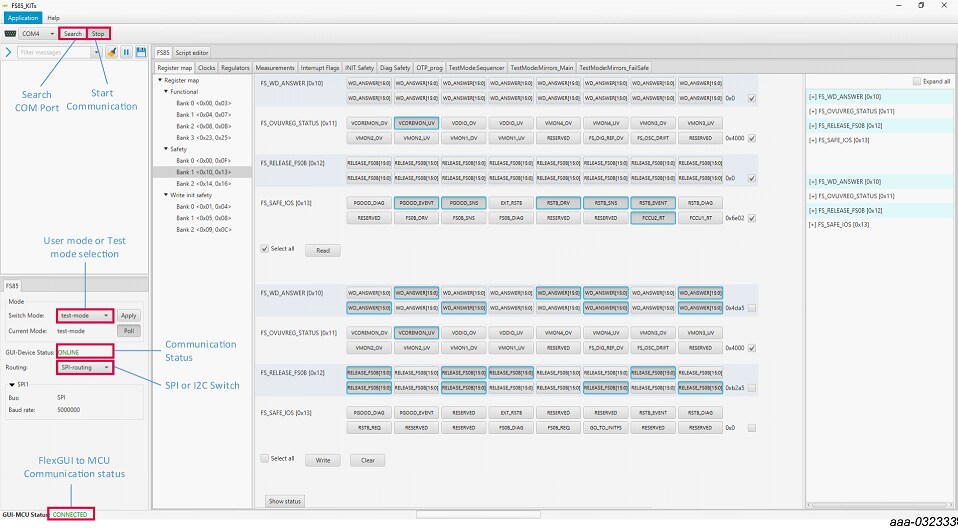
The image below shows the mode selection. At first launch, the FlexGUI starts in User mode. The user can then decide to switch to Test mode using the Switch mode drop-down list.
4.3 Complete step by step software instructions are detailed in the User Guide
Refer to UM11183.
Design Resources
Board Information
Software Information
Additional Resources
Product Summary Page
FS8400 : Safety System Basis Chip for S32 Microcontroller, fit for ASIL B
FS8500 : Safety System Basis Chip for S32 Microcontroller, fit for ASIL D
Tool Summary Page
The overview tab provides an overview of the device, product features, a description of the kit contents, a list of (and links to) supported devices, list of (and links to) any related products and a Get Started section.
- On the Overview tab, locate the Jump To navigation feature on the left side of the window.
- Select the Get Started link, review each entry and download an entry by clicking on the title.
-
After reviewing the Overview tab, visit the other product related tabs for additional information:
- Documentation: download current documentation
- Software and Tools: download current hardware and software tools / Drivers
- Buy/Parametrics: purchase the product and view the product parametrics
After downloading files, review each file, including the user guide, which includes setup instructions.
- Build package: the bill of materials (BOM) and supporting schematics are also available for download in the Get Started section of the Overview tab.
In addition to our FS8500/FS8400 Safety System Basis Chip for S32 Microcontrollers page you may also want to visit:
References
Product pages:
Application Pages:
Hardware pages:
Software pages:
Community page:
このページ
- 1.1
Kit contents/packing list
- 1.2
Kit contents
- 1.3
Additional hardware
- 1.4
Windows PC workstation
- 1.5
Software
- 1.6
User manual
- 2.1
Board features
- 2.2
KITFS85SKTEVM evaluation board features
- 2.3
Board Descriptions
- 2.4
Board Image
- 2.5
Additional board support
- 3.1
Configure the hardware
- 3.2
Configuration image
- 3.3
Device Considerations
- 3.4
Setting up the board
- 3.5
Additional Board Support