FRDM-A-S32K118開発ボードのスタート・ガイド
サインイン 進行状況を保存するには アカウントをお持ちでない方 アカウントを作成する。
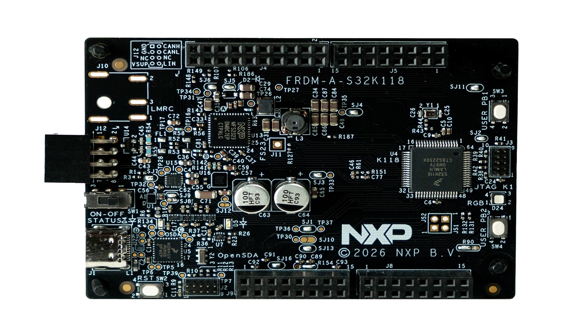
お客様の 車載向けFRDM S32K118開発ボード
1. パッケージの内容
NXPのFRDM-A-S32K118は、シンプルながらもパワフルなプラットフォーム上でS32K118車載グレード・マイクロコントローラ・ユニット (MCU) の性能を引き出せる、コスト効率に優れたボードです。FRDM-A-S32K118は、フル機能のS32K118EVB-Q064をベースとしており、車載、組込み、産業用システムのエンジニアはもちろん、趣味としてコンパクトで多用途の開発ソリューションを求めているユーザーにとっても最適なツールです。
このガイドでは、ハードウェアのコンポーネントとボードの構成について説明します。
1.1 キットの内容と同梱物一覧
FRDM-A-S32K118には以下のものが含まれています。
- FRDM-A-S32K118ボード
- USB Type-Cケーブル
- スタート・ガイド・ポストカード
- キット内容シート
2. ソフトウェアの入手
資格情報を使用してNXPにサインインします。
2.1 ソフトウェアのインストール
- FRDM Automotive Bundleのリンクからソフトウェア・バンドルへ移動します
- [Generate(生成)]をクリックしてダウンロードします
- NXP Multi Installerを実行します
- デスクトップに作成されたショートカットからS32 Design Studio for S32 Platform 3.6.5を起動します
「Launch executable after download(ダウンロード後に実行可能ファイルを起動する)」と「Installation and configuration without any interaction(操作を一切行わずにインストールおよび構成する)」を選択すると、FRDMバンドルと利用可能なすべてのコンポーネントが一緒にインストールされます。
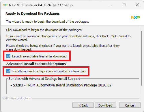
すべてのソフトウェアが自動でインストールおよび構成されました。
2. ハードウェアの入手
このセクションでは、FRDM-A-S32K118ボードのコンポーネントと機能について説明します。
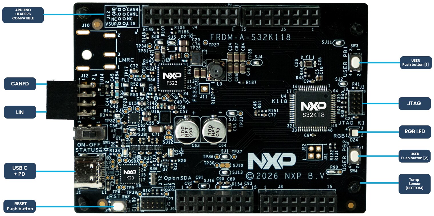
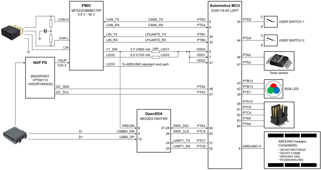
3.1 ボードの特長
- 以下の製品を使用した給電機能
- NX20P0407
- PTN5110
- NX20P3483UK
- システムベーシス・チップ (SBC) FS23
- 故障検出および制御ユニット (FCCU) セーフティ・ピン
- FS23の組込み5 Mbコントローラ・エリア・ネットワーク (CAN)
- 組込みローカル・インターコネクト・ネットワーク (LIN)
- Kinetis K20を使用したOpenSDA(オープン・スタンダード・シリアル/デバッグ・アダプタ)デバッグ・インターフェース
- S32K118車載用MCU 100 LQFP
- 10ポジション、0.050インチ (1.27 mm)、表面実装JTAG (Joint Test Action Group) コネクタ・ヘッダ
- デバッグのための2個のユーザー用プッシュ・ボタン
- RGB LED
- PCT2075D温度センサ
- 以下の製品とのピン互換性:
- Arduino® UNO
- PCA9958HN-ARD
- DEVKIT-MOTORGD
- DEVKIT-COMM
3. ハードウェアの構成
このセクションでは、FRDM-A-S32K118ボードのセットアップ手順を説明します。設定の詳細については、以下の表を参照してください。
4.1 デフォルト設定
| インターフェース | 参照/信号 | デフォルト設定 | コメント |
|---|---|---|---|
| NXP給電製品 | U1 |
NX20P0407 | NX20P0407は、Configuration Channelピン (CC1/CC2) およびSideband Useピン (SBU1/SBU2) へのスマート過電圧保護として機能し、バス電圧 (VBUS) の給電 (PD) を制御して、USB-Cと外部ソース間の安全で効率的な電力パス切り替えを確保します。 |
U15 |
PTN5110 | PTN5110は、USB Type-C通信を管理するためのUSB PD物理層 (PHY) として機能し、電圧と必要な電流のネゴシエーションを行います。 | |
U16 |
NX20P3483UK | NX20P3483UKは、USB-Type Cアプリケーションの電源スイッチとして使用され、PO回路を保護します。 | |
USBC_I2C_SCL |
PTA3 | MCU (S32K118) からPHY (PTN5110) へのPOのネゴシエーションに使用されるI²Cクロック信号。 | |
USBC_I2C_SDA |
PTA2 | MCU (S32K118) からPHY (PTN5110) へのPOのネゴシエーションに使用されるI²Cデータ信号。 | |
| FS23 | U13 |
MFS2323BMBA5EP | このバージョンのFS23は、2つの低ドロップアウト・レギュレータ (LDO) に加えてDC-DCレギュレータを搭載しており、さまざまなペリフェラルの包括的なパワー・マネジメントを提供します。さらに、このバージョンにはCANおよびLIN PHYが内蔵されています。 |
CANH |
J12 - 2 |
FS23から供給されるコントローラ・エリア・ネットワークのハイ (CANH) 信号。 | |
CANL |
J12 - 4 |
FS23から供給されるコントローラ・エリア・ネットワークのロー (CANL) 信号。 | |
LIN |
J12 - 8 |
FS23から供給されるLIN信号。 | |
SJ4 |
• | FS23に内蔵されたDC-DCコンバータからの5.0 V出力電圧。 | |
SJ6 |
• | FS23 LDO2からの3.3 V出力電圧。 | |
SJ7 |
• | FS23 LDO3からの5.0 V出力電圧。 | |
| OpenSDA | U5 |
MK20DX128VFM5 | S32K118に接続されたオンボード・デバッグ・インターフェース。 |
| MCU | U4 |
S32K118 | ASIL BシングルArm® Cortex®-M4 @ 80 MHz(HS-RUNモードのMCUでは112 MHz)および2 MB汎用MCU。 |
| JTAG | J3 |
• | S32K118 MCUのJTAGインターフェースは、10ピン、1.27 mmヘッダを介して接続。 |
| ユーザー用RGB LED | D24 |
PTB12 - FTM0_CH0 | 青色、アクティブ・ハイ。 |
- |
PTB13 - FTM0_CH1 | 緑色、アクティブ・ハイ。 | |
- |
PTE7 - FTM0_CH7 | 赤色、アクティブ・ハイ。 | |
| ユーザー用プッシュ・ボタン | SW3 |
PTD5 | 汎用。 |
SW4 |
PTD4 | 汎用。 | |
| 温度センサ | U18 |
PCT2075D | -25°C~+100°Cの温度範囲で±1°Cの精度を実現するI²C温度-デジタル・コンバータ。LM75のピン互換置換品。 |
4.2 はんだブリッジ・ジャンパの設定
| インターフェース | 参照/信号 | デフォルト設定 | コメント |
|---|---|---|---|
| 給電 | SJ3 |
• | 電源スイッチ (U16) からの出力をFS23の入力に接続するために使用されるはんだブリッジ。 |
SJ8 |
• | USB Type-Cポートを保護するためのはんだブリッジ。 | |
SJ9 |
- | USB Type-Cポートを保護するための未実装の補助的はんだブリッジ。 | |
SJ12 |
- | USB Type-C電源スイッチの5.5 Vピンに電源を供給するために使用される未実装のはんだブリッジ。 | |
| FS23 | R45 |
1 - 2 | USB Type-C電源または電源ジャックのセレクタとして使用されるはんだブリッジ。 |
SJ4 |
• | PMICのDC/DC降圧コンバータからの出力をボード全体の電源供給に接続するために使用されるはんだブリッジ。出力電圧は5 Vです。 | |
SJ5 |
• | ダイオードの保護なしでFS23のLDO2からの出力をバイパスするために使用されるはんだブリッジ。 | |
SJ6 |
• | PMICのLDO2からの出力をボード全体の電源供給に接続するために使用されるはんだブリッジ。出力電圧は3.3 Vです。 | |
SJ7 |
• | PMICのLDO3からの出力をボード全体の電源供給に接続するために使用されるはんだブリッジ。出力電圧は3.3 Vです。 | |
| OpenSDA | SJ15 |
• | FS23のV1からのMK20の入力電圧を選択するためのはんだブリッジ。 |
SJ14 |
- | FS23のV3からのMK20の入力電圧を選択するためのはんだブリッジ。 | |
SJ1 |
• | MCUからのVDD電源を、オンボード・デバッガMK20からS32K1への信号のインターフェースとなる電圧変換器に接続するために使用されるはんだブリッジ。 | |
| MCU | SJ10 |
• | PMICのV1からの電圧をS32K1に接続するために使用されるはんだブリッジ。 |
SJ13 |
- | PMICのV2からの電圧をS32K1に接続するために使用されるはんだブリッジ。 | |
| JTAG | SJ2 |
• | JTAGコネクタに電源を供給するために使用されるはんだブリッジ。 |
| Arduino | R153 |
1 - 3 | PMICからArduinoコネクタの3.3 Vリファレンスへのリファレンス電圧を選択するために使用されるはんだブリッジ・セレクタ。 |
R154 |
1 - 3 | PMICからArduinoコネクタの5.0 Vリファレンスへのリファレンス電圧を選択するために使用されるはんだブリッジ・セレクタ。 | |
SJ1 |
• | PTA2をJ5-3に接続するため、またはJS2を使用してPTA2をJ5-1に接続するための外部1x2ヘッダ (HDR) を搭載するために使用されるはんだジャンパ。 |
|
SJ2 |
• | PTA3をJ5-1に接続するため、またはJS2を使用してPTA3をJ5-3に接続するための外部1x2 HDRを搭載するために使用されるはんだジャンパ。 |
|
| ユーザー・ペリフェラル | SJ11 |
• | ボードのペリフェラル・セクションを有効化するために使用されるはんだブリッジ。 |
R90 |
1 - 3 | RGB LEDへの電源供給として3.3 Vまたは5 Vを選択するために使用されるはんだブリッジ。 |
設計・リソース
ボードに関するドキュメント
サポート
トレーニング
フォーラム
NXPのコミュニティ・サイトで、他のエンジニアとつながり、FRDM-A-S32K118開発ボードを使用した設計に関する専門的なアドバイスを受けることができます。