ZigBee and IEEE802.15.4 Wireless Microcontroller with 512 KB Flash, 32 KB RAM
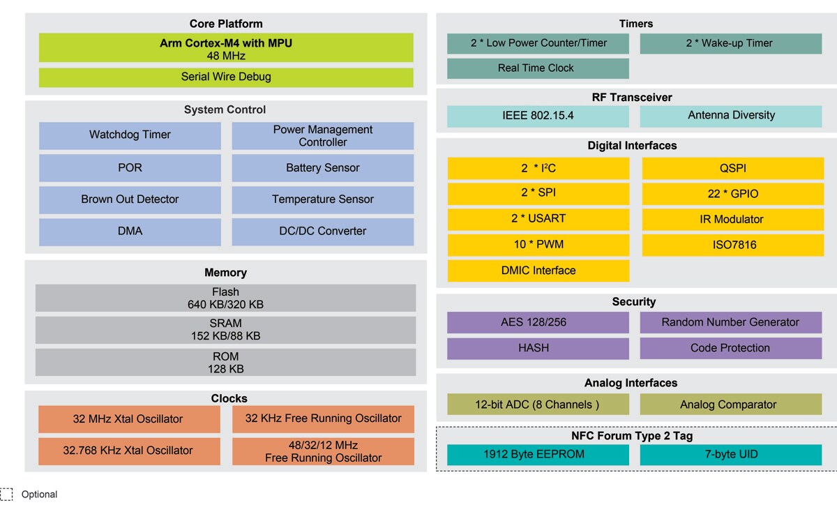
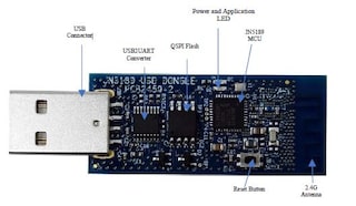
The JN5189 portfolio is designed to power the next generation of very low current wireless devices, supporting Zigbee 3.0, Thread, and IEEE 802.15.4. It includes several low-power modes and ultra-low TX and RX power consumption, which enables devices powered by JN5189/88 to have a longer battery life. With -100 dBm RX sensitivity and up to +11 dBm TX output power, JN5189/88 offers reliable and robust communications performance.JN5189/88 is powered by an Arm® Cortex®-M4 MCU and can run up to 640 KB onboard flash and 152 KB SRAM, with enough room and flexibility for complex applications and OTA upgrade capability without external memory. It has a rich set of MCU peripherals and multiple serial communication interfaces for embedded connected applications. JN5189T/88T has an integrated NFC NTAG to implement contactless NFC commissioning, simplifying the network build-out.
ZigBee and IEEE802.15.4 Wireless Microcontroller with 512 KB Flash, 32 KB RAM
|
|
|
|
|
|
|
|---|---|---|---|---|---|
|
|
|
|
|
|
|
|
|
|
|
|
|
|
|
|
|
|
|
|
|
|
|
|
|
|
|
|
|
|
|
|
|
|
|
|
|
|
|
|
|
|
|
|
|
|
|
|
|
|
|
|
|
|
|
|
|
|
|
|
|
|
|
|
|
|
|
|
|
|
クイック・リファレンス ドキュメンテーションの種類
1-10 件/全 28 ドキュメント
コンパクトリスト
2 設計・ファイル
完全な内訳を受け取ります。 製品の設置面積などについては、 eCad ファイル.
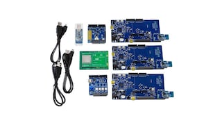
1-5 件/全 8 ハードウェア提供
クイック・リファレンス ソフトウェア・タイプ.
1-5 件/全 11 ソフトウェア・ファイル
追加ソフトウェアを利用可能 パートナー・ソリューションの特集を表示.
注: より快適にご利用いただくために、ソフトウェアのダウンロードはデスクトップで行うことを推奨します。
NXPから直接サポートを受けるには、以下のサイトをご覧ください。 エンジニアリング・サービス.
1 エンジニアリング・サービス

この製品をサポートするその他のパートナー製品を見つけるには、当社の Web サイトにアクセスしてください パートナーマーケットプレイス.