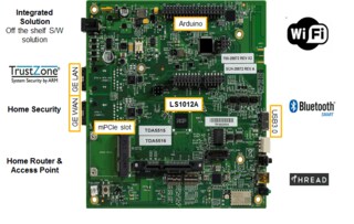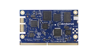

Layerscape® 1012A Low Power Processor
デザイン・ファイル
完全な内訳を受け取ります。 製品の設置面積などについては、 eCad ファイル.
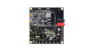
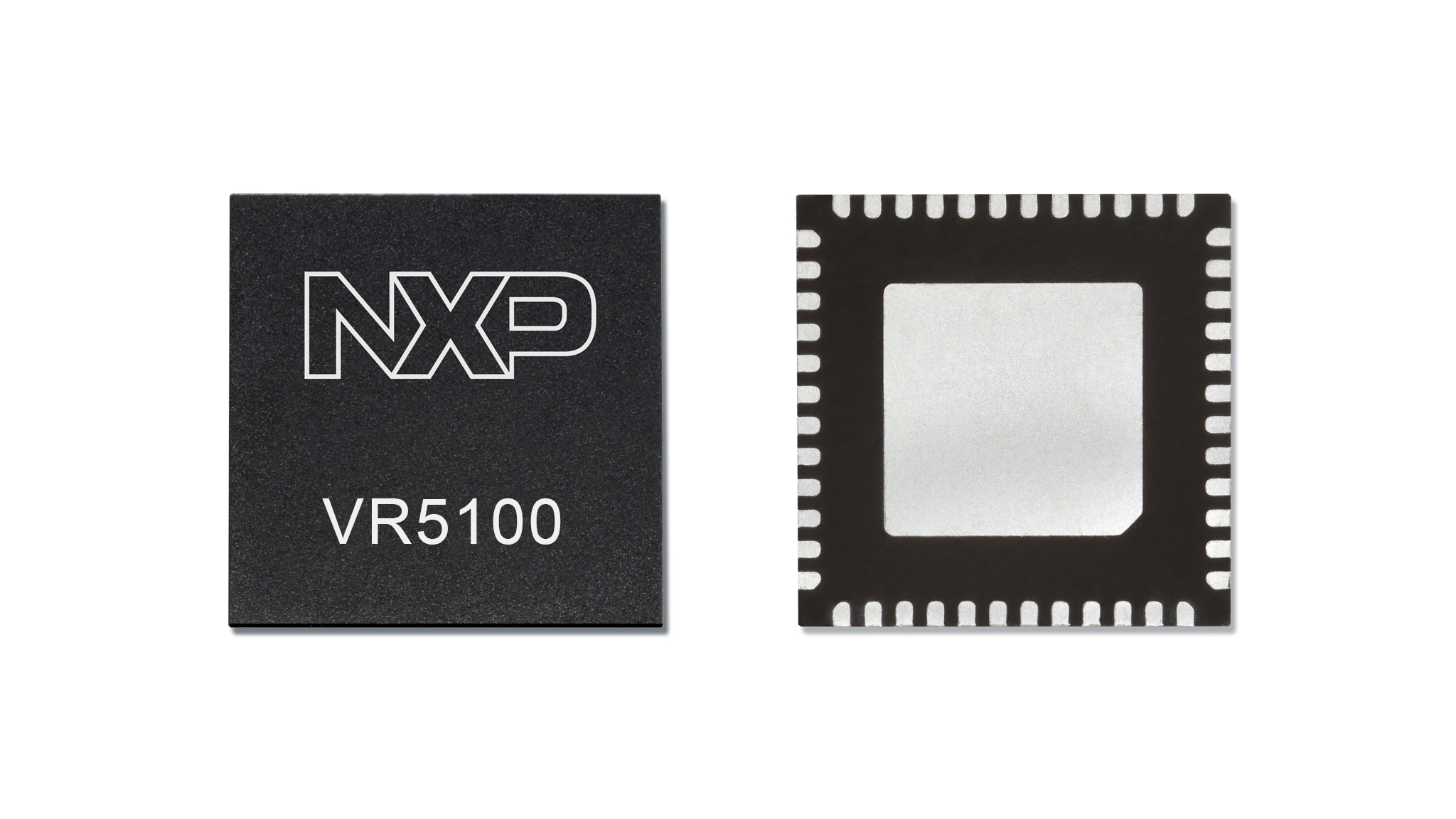
The VR5100 is a high performance, multi-output DC-DC regulator designed to power single or dual core LS1 processors like LS1012A and LS1024A. It includes three buck regulators, six LDOs and a boost regulator offering a complete power management solution for Network Attached Storage, battery operated Mobile NAS, IoT gateway, Home and factory automation systems.
The VR5100 uses a low quiescent current architecture allowing high efficiency operation at light load extending the battery life. The high frequency operation reduces the total solution to less than 0.5 sqin. The high power QFN package keeps the junction temperature low even at high ambient temperature.
|
|
|
|
|
|
|
|---|---|---|---|---|---|
|
|
|
|
|
|
|
|
|
|
|
|
|
|
|
|
|
|
|
|
|
|
|
|
|
|
|
|
|
|
|
|
|
|
|
|
|
|
|
|
|
|
|
|
|
|
|
|
|
|
|
|
|
|
|
|
|
|
|
|
|
|
|
|
|
|
|
|
|
|
クイック・リファレンス ドキュメンテーションの種類
6 ドキュメント
コンパクトリスト
完全な内訳を受け取ります。 製品の設置面積などについては、 eCad ファイル.
NXPから直接サポートを受けるには、以下のサイトをご覧ください。 エンジニアリング・サービス.
2 エンジニアリング・サービス

この製品をサポートするその他のパートナー製品を見つけるには、当社の Web サイトにアクセスしてください パートナーマーケットプレイス.