PF09パワー・マネジメントIC評価ボードのスタート・ガイド。
このドキュメントの内容
-
パッケージの内容
-
ハードウェアについて
-
ハードウェアの構成
サインイン 進行状況を保存するには アカウントをお持ちでない方 アカウントを作成する。
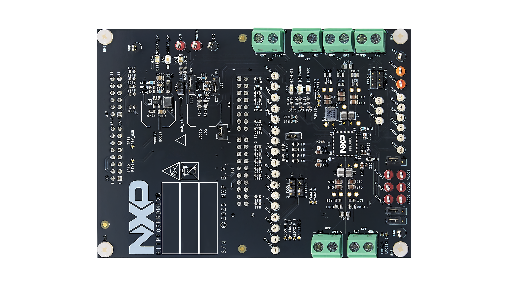
お客様の PF09評価ボード
1. パッケージの内容
NXPのアナログ製品開発ボードは、NXP製品の評価を目的とした使いやすいプラットフォームです。さまざまなアナログ・ソリューション、ミックスド・シグナル・ソリューション、パワー・ソリューションに対応しています。実績のある大容量テクノロジを使用したモノリシック集積回路およびシステム・イン・パッケージ (SiP) デバイスを搭載しています。NXP製品は、最先端システムへの電源供給において、より長いバッテリー寿命、より小さいフォーム・ファクタ、より少ない部品数、より低いコスト、改善されたパフォーマンスを実現します。
このページでは、KITPF09FRDMEVMボードをセットアップして使用する手順について説明します。
1.1 キットの内容/同梱物一覧
KITPF09FRDMEVBを使用するには、キットの同梱物と追加のハードウェアに加え、ソフトウェアがインストールされたWindows PCワークステーションが必要です。
キットには以下のものが含まれています。
- 組立ておよびテスト済み評価ボードとプログラム済みKL25Zマイクロコントローラ(静電気防止バッグ入り)
- 3.0フィートのUSB-STD A to USB-B-microケーブル
- Phoenixコネクタ(2ポジション、ストレート、10 mm)x 6
- ボードに搭載されたジャンパ
- クイック・スタート・ガイド
1.2 追加ハードウェア
このボードの作業をする際は、キットの内容物のほかに以下のハードウェアが必要になるか、または使用すると役立ちます。
- 5 Vを供給可能な電源
1.3 最小システム要件
この評価ボードにはWindows PCワークステーションが必要です。この評価ボードで作業する際は、これらの最低限の仕様を満たすことで良好な結果が得られます。
- Windows 7またはWindows 10を搭載したUSB対応のコンピュータ
- FTDI USBシリアル・ポート・ドライバ(FT230X基本UARTデバイス用)
1.4 ソフトウェア
KITPF09FRDMEVB評価ボードで作業するには、ソフトウェアのインストールが必要です。記載されているすべてのソフトウェアは、PF09:高性能アプリケーション用9チャネルPMIC、ASIL DおよびSIL 2のページにある評価ボードの情報ページ、または提供されているリンクから入手できます。
- 車載ファミリ用NXP GUIインストール・パッケージ:最新バージョン
2. ハードウェアについて
2.1 ボードの特長
- 電源入力用Phoenix (10 mm) オス・コネクタまたはジャック・コネクタ
- PMICスイッチャ出力用Phoenix (10 mm) オス・コネクタ
- I/O構成用ヘッダ・コネクタ
- プログラミング用の選択可能な電源入力
- 入出力へのアクセス用のアクセス・ピン・コネクタ
- 信号またはレギュレータの状態を示す赤色と緑色のLEDインジケータ
- 8 VのOTP書き込み電圧が設定されていることを示す青色LED
- KL25Z MCUによる高度なシステム監視
- 組込みUSB to I²CプロトコルによりKL25Z MCUを介したソフトウェアGUIへの接続が容易
2.2 ボードの説明
キットのハードウェアは、KL25Zマイクロコントローラが組み込まれたKITPF09FRDMEVB評価ボードと、ボードをPCに接続するためのUSBケーブルで構成されています。
KITPF09FRDMEVB評価ボードは、追加のツールなしで、デバイスに備わる2回プログラム可能な (OTP) 機能を使用して、ユーザーが個々のPF09ファミリをヒューズ書き込みできるソケットを備えています。ボード上のコネクタ、ジャンパ、スイッチを使用して、特定の設計要件を満たした評価環境を構成できます。このボードに搭載されたLEDとテスト・ポイントを使用して、リアルタイムでパフォーマンスを監視することもできます。ユーザーは、デバイスをプログラミングする前に、エミュレーション・モードで必要な数の構成をテストすることが可能です。
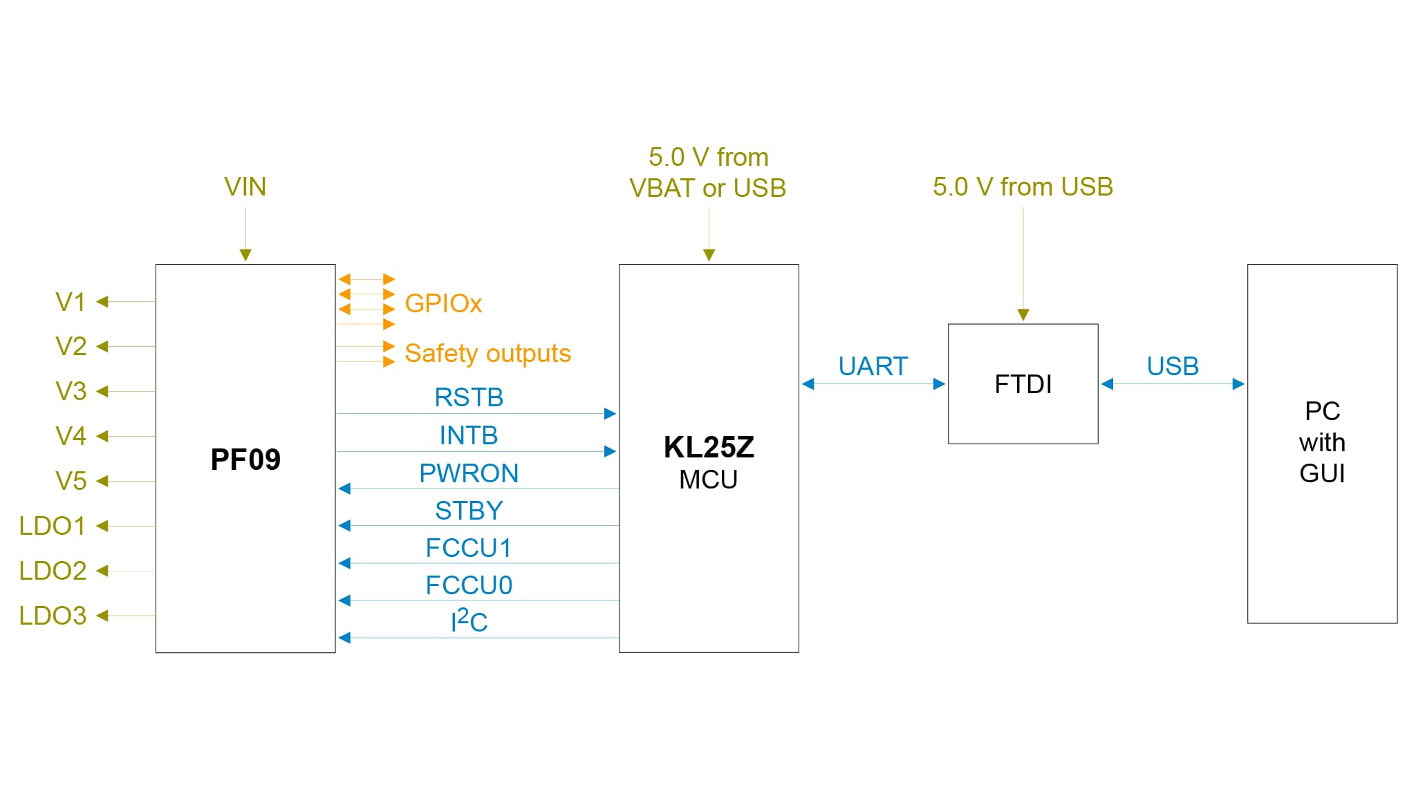
KL25Zは、KITPF09FRDMEVBボードの裏側にはんだ付けされています。KL25Zの役割は、KITPF09FRDMEVBボードとPCにインストールされたGUIとの間のI²C通信を管理することです。KL25Zは、PCに接続されたUSBケーブルまたはバッテリー電源(GUIに接続されていない場合)から電力を取り込みます。
3. ハードウェアの構成
3.1 ハードウェアの構成
KITPF09FRDMEVB評価ボードの設定手順は次のとおりです。
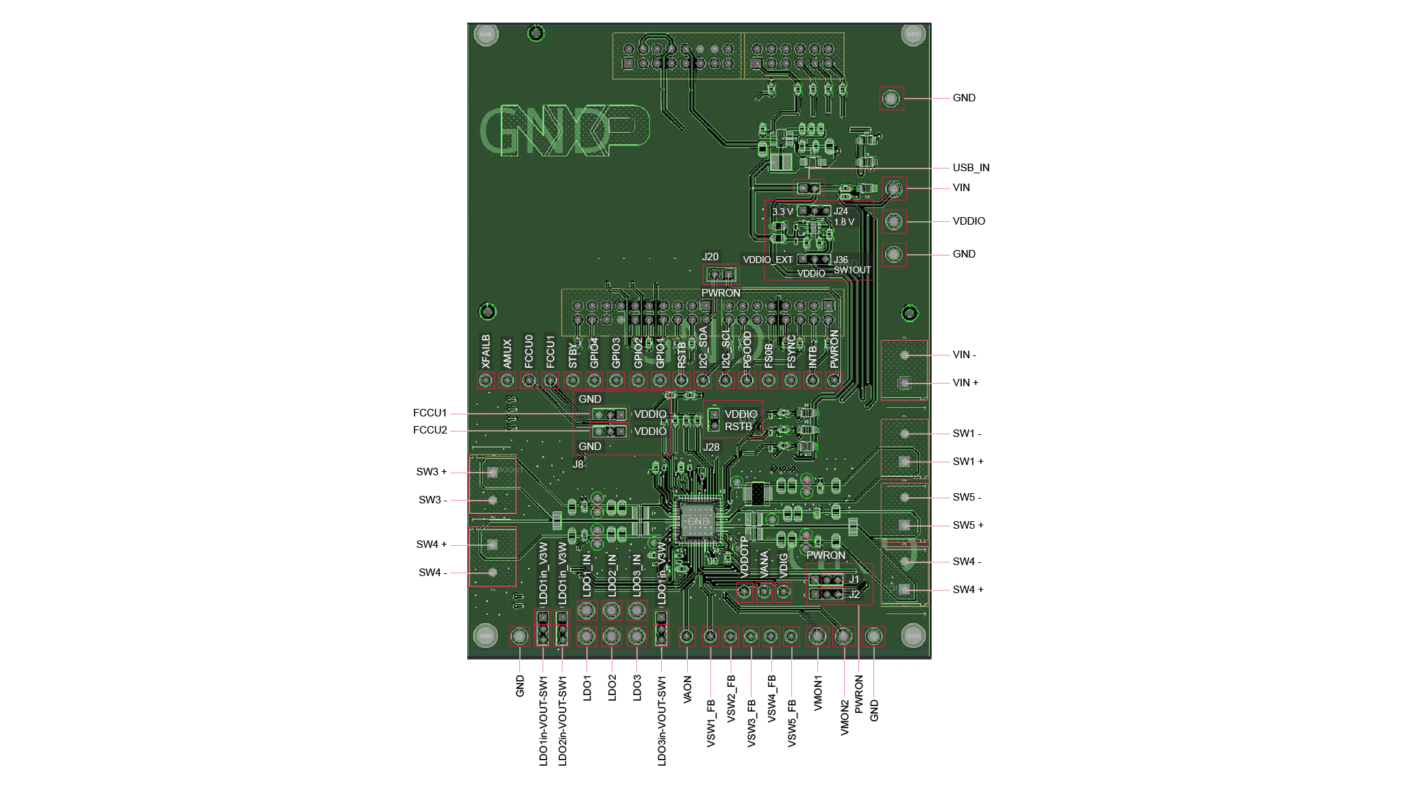
- ボードのジャンパとスイッチがデフォルト位置に設定されていることを確認します。このデフォルトのデバッグ構成により、KL25Z MCU(I²C経由)およびGUIによるボードの完全な制御が可能になります。セクション4.4では、PF09ファミリのデフォルトのジャンパおよびスイッチの設定を示しています。
- 電源をVIN-J47(Phoenixコネクタ - 10 mm)に接続します。電源は公称値5 Vに設定する必要があります。
- ボードとPC間のUSBケーブルが確実に接続されていることを確認してください。この接続は、極めて重要となります。USBポートはPCとオンボードのKL25Z MCU間の通信チャネルとして機能し、一部のオンボード回路に電圧とリファレンスも供給するためです。
このデフォルトのデバッグ構成により、KL25Z MCU(I²C経由)およびGUIによるボードの完全な制御が可能になります。図2は、PF09のデフォルトのジャンパおよびスイッチの設定を示しています。PF09のデフォルトのジャンパおよびスイッチの設定については、以下を参照してください。
| 参照 | 説明 | 構成用の設定 | 外部構成 | |
|---|---|---|---|---|
J1 |
PWRONプルアップ電圧の選択 |
ピン:1-2 | VIN |
開 |
| ピン:2-3 | VAON |
開 | ||
J2 |
VDDOTPの接続 |
ピン:1-2 | VDIG |
開 |
| ピン:2-3 | VDDOTP_BST |
接続済み | ||
J9 |
FCCU0入力レベルの接続 |
ピン:1-2 | VDDIO |
--- |
| ピン:2-3 | GND |
--- | ||
J10 |
FCCU1入力レベルの接続 |
ピン:1-2 | VDDIO |
--- |
| ピン:2-3 | GND |
--- | ||
J20 |
インターフェース・システムへのパワーオン接続 | ピン:1-2 | 接続済み | 接続済み |
J24 |
外部VDDIO電圧の選択(1-2:1.8 V <-> 2-3:3.3 V) |
ピン:1-2 | 1.8 V | --- |
| ピン:2-3 | 3.3 V | 接続済み | ||
J29 |
VDDIOへのRSTBプルアップ、動作時に接続 |
ピン:1-2 | 接続済み | 接続済み |
J36 |
VDDIO電源入力の注入 |
ピン:1-2 | 外部 | 接続済み |
| ピン:2-3 | SW1 |
--- | ||
J48 |
LDO1入力電圧 |
ピン:1-2 | VSW_IN |
接続済み |
| ピン:2-3 | SW1_OUT |
--- | ||
J49 |
LDO2入力電圧 |
ピン:1-2 | VSW_IN |
接続済み |
| ピン:2-3 | SW1_OUT |
--- | ||
J50 |
LDO3入力電圧 |
ピン:1-2 | VSW_IN |
接続済み |
| ピン:2-3 | SW1_OUT |
--- | ||
J54 |
USBジャンパ。USB電源に接続する場合に使用。外部電源 (VIN) を使用する場合は「開」。正しく動作するように外部電源を接続します |
ピン:1-2 | 使用 - USB電源 開 - 外部電源 |
開 |
| 参照 | 機能 | 説明 |
|---|---|---|
J39 |
SW2出力 |
PMICスイッチャ2出力電圧。PMICピンへの直接接続 |
J40 |
SW3出力 |
PMICスイッチャ3出力電圧。PMICピンへの直接接続 |
J41 |
SW4出力 |
PMICスイッチャ4出力電圧。PMICピンへの直接接続 |
J42 |
SW5出力 |
PMICスイッチャ5出力電圧。PMICピンへの直接接続 |
J43 |
SW1出力 |
PMICスイッチャ1出力電圧。PMICピンへの直接接続 |
J47 |
VIN |
入力電圧は電源から供給可能。供給範囲:3.3 V~5.0 V(仕様に応じて) |
| 参照 | 機能 | 説明 | 色 |
|---|---|---|---|
BH1 |
GND |
ボードのグランドの直接接続 - 4つの容易なアクセス・ポイント | 黒 |
BH2 |
|||
BH3 |
|||
BH4 |
|||
TP119 |
LDO1IN |
LDO1入力電圧のモニタリング・ポイント |
赤 |
TP120 |
LDO2IN |
LDO2入力電圧のモニタリング・ポイント |
赤 |
TP121 |
LDO3IN |
LDO3入力電圧のモニタリング・ポイント |
赤 |
TP61 |
VLDO1 |
LDO1出力のモニタリング・ポイント |
赤 |
TP60 |
VLDO2 |
LDO2出力のモニタリング・ポイント |
赤 |
TP59 |
VLDO3 |
LDO3出力のモニタリング・ポイント |
赤 |
TP15 |
VAON |
VAON出力のモニタリング・ポイント |
白 |
TP90 |
SW1 FB |
SW1フィードバックのモニタリング・ポイント |
白 |
TP86 |
SW2 FB |
SW2フィードバックのモニタリング・ポイント |
白 |
TP87 |
SW3 FB |
SW3フィードバックのモニタリング・ポイント |
白 |
TP91 |
SW4 FB |
SW4フィードバックのモニタリング・ポイント |
白 |
TP92 |
SW5 FB |
SW5フィードバックのモニタリング・ポイント |
白 |
TP78 |
VMON1 |
外部モニタVMON1のモニタリング・ポイント |
オレンジ |
TP79 |
VMON2 |
外部モニタVMON2のモニタリング・ポイント |
オレンジ |
TP65 |
XFAILB |
XFAILB PMICアクセス・ポイント - 双方向ピン |
白 |
TP57 |
GPIO1 |
GPIO1アクセス・ポイント - 双方向ピン |
白 |
TP20 |
GPIO2 |
GPIO2アクセス・ポイント - 双方向ピン |
白 |
TP56 |
GPIO3 |
GPIO3アクセス・ポイント - 双方向ピン |
白 |
TP8 |
GPIO4 |
GPIO4アクセス・ポイント - 双方向ピン |
白 |
TP4 |
I²C-SDA |
I²C SDAアクセス・ポイント - 双方向ピン |
白 |
TP5 |
I²C-SCL |
I²C SCLアクセス・ポイント - 双方向ピン |
白 |
TP9 |
FSYNC |
FSYNCアクセス・ポイント - 双方向ピン |
白 |
TP55 |
AMUX |
アナログ・マルチプレクサ出力モニタリング・ポイント | 白 |
TP12 |
RSTB |
システム・リセット信号出力モニタリング・ポイント | 白 |
TP3 |
FS0B |
フェイルセーフ出力モニタリング・ポイント | 白 |
TP10 |
INTB |
INTB出力モニタリング・ポイント |
白 |
TP52 |
FCCU0 |
FCCU0フォルト・モニタリング入力ピン・アクセス・ポイント |
白 |
TP53 |
FCCU1 |
FCCU1フォルト・モニタリング入力ピン・アクセス・ポイント |
白 |
TP6 |
STBY |
STBY入力ピン・アクセス・ポイント |
白 |
TP2 |
PGOOD |
PGOOD入力ピン・アクセス・ポイント |
白 |
TP7 |
PWRON |
パワーオン入力ピン・アクセス・ポイント | 白 |