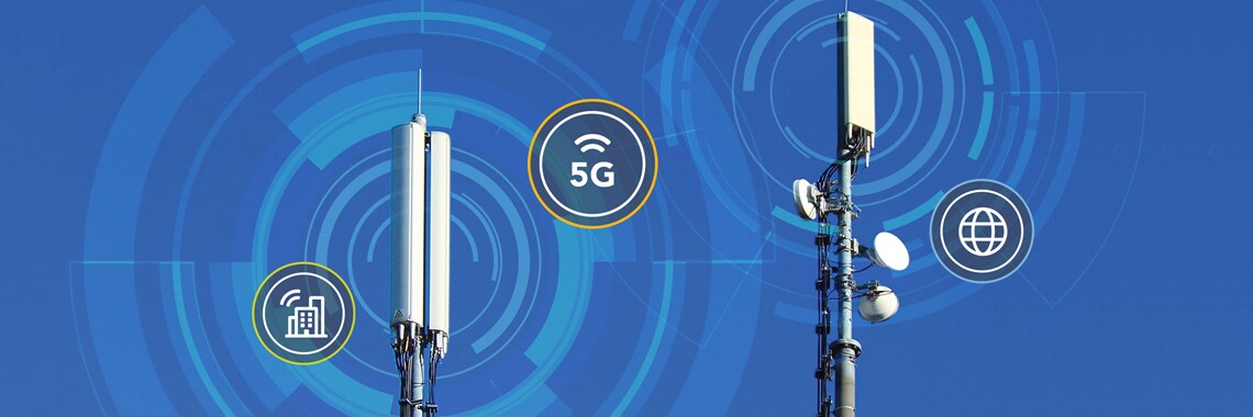
Each new generation of cellular brings with it a new set of challenges and 5G is on a different scale. The arrival of
5G is a comprehensive technology shift not just for semiconductors but for the industry as a whole.

We are moving to the future. 5G is designed to be both broader in scope and technologically more complex than
preceding generations of cellular. Many of 5G’s most advanced capabilities are still on the horizon, but now is the
time to prepare for its arrival. That means that as semiconductor manufacturers, we are already deep into the
details of how best to meet future requirements.
NXP strives by anticipating change and optimizing for new cellular requirements. For as long as there’s been a
cellular industry, we have been building and refining advanced processing technologies.
As we enter the 5G era, we see the need for a different approach. This is especially true when it comes to 5G
infrastructure equipment like base stations. Base stations present a very specific set of requirements for
successful 5G operation. Our work in Gallium Nitride (GaN), a relative newcomer to cellular, shows us that GaN is
the way to make the 5G infrastructure come alive.
GaN Enables 5G
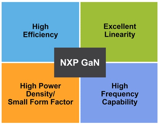
LDMOS processes have dominated in base stations for some time now, but LDMOS is reaching the limits of what it can
do. GaN is just now getting started—already meeting today's demanding 5G requirements but also allowing significant
room for improvements and extensions for future generations of GaN.

What GaN can do for 5G today and tomorrow is a big reason why the GaN market is expected to grow quickly. The French
analyst firm Yole Development, which specializes in emerging markets and RF devices and technologies, predicts that
the total GaN RF market will be above USD 2 billion by 2025 with a 12% CAGR between 2019 and 2025. This prediction
includes both 5G infrastructure and defense applications.
NXP’s Big Investment in GaN for 5G
With the celebration of ‘Happy GaNuary’ this month, at NXP we’re all in for GaN and 5G. Our GaN portfolio already
offers exceptional performance and efficiency and continues to expand support for all frequencies and power levels.
Our focus is on the range at and above 2 GHz, since that’s where the highest-performing 4G and 5G applications
operate.
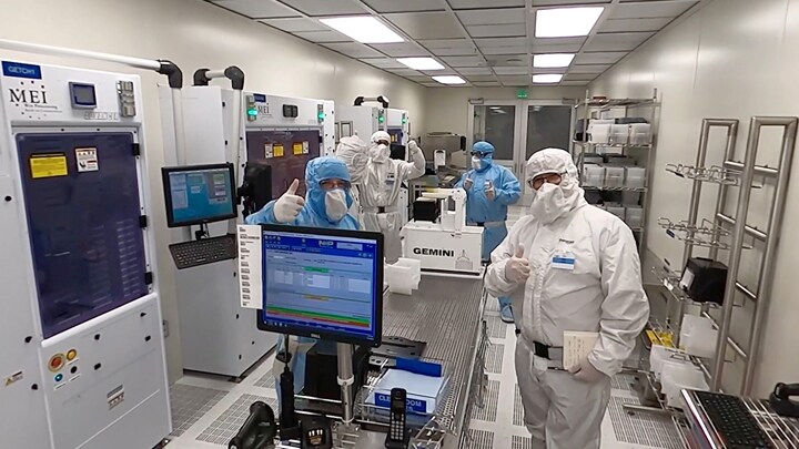
We haven’t stopped there! The real news is that NXP has achieved a first for GaN by building a state-of-the-art GaN
manufacturing facility in the United States that supports the specific needs of 5G operations.
On September 29, 2020 NXP celebrated the Chandler GaN fab grand opening and is ramping up into high volume production
now!
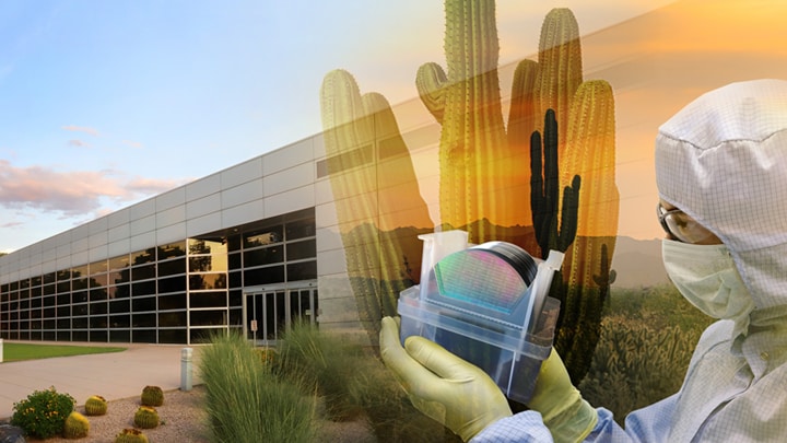
In order to create the new facility, we started with our legacy fab in Chandler, Arizona (an electroplating line for
automotive) and converted it to a six-inch (150 mm) wafer size RF GaN fab. Our GaN fab is the only in the world
today that adheres to automotive quality standards, which are often higher than those used by other industries.
The new GaN facility draws on the expertise of our process engineers. These engineers have worked extensively with
Gallium Arsenide (GaAs) and build on the legacy of the Motorola GaAs factory in Tempe, which was at one time the
largest in the world. In creating the Chandler GaN fab, our engineers and technology experts drove to understand our
cellular customer requirements. These engineers and experts had worked closely to determine ways that the RF portion
of the design needs to interact with digital-control systems.
The Chandler GaN fab joins our other foundries for telecom, including our RF LDMOS line. Bringing GaN production
in-house makes sense for a number of reasons. We’ve been involved with GaN since 2003, working with both internal
and external foundries for many years. Building and running our own fab gives us more control over the process, with
a closer connection between the fab and the research and development team.
Having GaN in-house also gives us more control over our roadmap, which includes continuous innovation and regular
upgrade introductions that deliver even higher levels of efficiency, size and cost. Our work in Chandler has already
yielded several valuable insights into how GaN can be optimized and enhanced.
Along with our considerable investment in the Chandler facility, we’re also adding talent and expanding our GaN
expertise. Having an advanced GaN facility also represents a significant contribution to U.S. efforts centered on
building a homegrown 5G infrastructure supply chain and establishing technology autonomy in 5G.
Just One Part of Our 5G Work
The Chandler GaN fab opening comes on the heels of another major 5G announcement in the U.S. Verizon
chose our Flexible Layerscape Access architecture for fixed wireless access (FWA). This is the first phase
of the migration from 4G LTE to 5G.
Our investment in Chandler also highlights our long-term commitment to 5G, which extends across our company. From 5G
modems and network processors to front-end components, base stations, mmWave products and receiver components. We’re
proactive to make 5G a reality.
To celebrate the ‘Happy GaNuary’ new year and learn more about our Chandler GaN facility and work in 5G, visit NXP RF GaN Fab Opening.