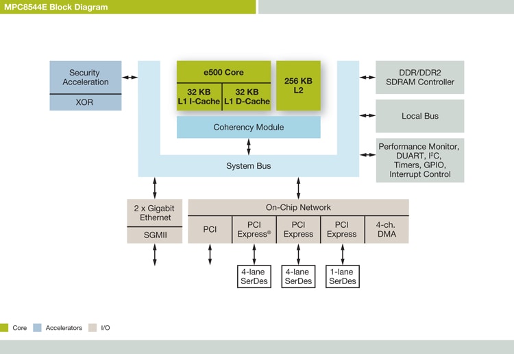
The MPC8544E PowerQUICC® III is designed to offer the unique combination of high performance, exceptional integration and lower overall power consumption required for networking, communications and industrial control applications.
The MPC8544E includes a high-performance e500 processor core built on Power Architecture® technology, enhanced peripherals and high-speed interconnect technology to balance processor performance with I/O system throughput enabling clock speeds scaling from 667 MHz up to 1.067 GHz. Third-generation PowerQUICC III processors are based on NXP®.s 90 nanometer (nm) silicon-on-insulator (SOI) copper interconnect process technology, which is designed to enable the processors to deliver higher performance with lower power dissipation.
The MPC8544E processor offers a wide range of high-speed connectivity options, including Gigabit Ethernet (GbE) interfaces with SGMII support and multiple PCI Express® connections. Support for these high-speed interfaces should enable scalable connectivity to network processors and/or ASICs in the data plane while the PowerQUICC III is designed to handle complex, computationally demanding control plane processing tasks. The MPC8544E is also designed to provide support for legacy PowerQUICC III interfaces such as PCI, I²C, dual universal asynchronous receiver/transmitters (DUART) and local bus connections. These processors are also designed to feature a next-generation double data rate (DDR2) memory controller, enhanced GbE support, v2 e500 double precision floating point and the field proven 90 nm PowerQUICC III integrated security engines.
Key Advantages
- High level of integration and performance
- Consistent programming model across the PowerQUICC III family
- Flexible SoC platform for fast time to market
- Simplified board design
- Large L2 cache at 256 KB
- High internal processing bandwidth
- Integrated DDR and DDR2 memory controller
- Two integrated Ethernet controllers (enhanced TSEC) with SGMII support
- Large L2 cache at 256 KB
- Flexible high-speed interconnection interfaces/multiple PCI Express connections
- 32-bit PCI support
- Integrated security engine
Access to the errata document for this device requires an NDA. Contact your local NXP Sales Office or NXP Authorized Distributor.