KITPF0300FRDMEVM評価ボードのスタート・ガイド
このドキュメントの内容
-
パッケージの内容
-
ハードウェアについて
-
ハードウェアの構成
サインイン 進行状況を保存するには アカウントをお持ちでない方 アカウントを作成する。
お客様の KITPF0300FRDMEVM
1. パッケージの内容
NXPのアナログ製品開発ボードは、NXP製品の評価を目的とした使いやすいプラットフォームです。さまざまなアナログ・ソリューション、ミックスド・シグナル・ソリューション、パワー・ソリューションに対応しています。実績のある大容量テクノロジを使用したモノリシック集積回路およびシステム・イン・パッケージ (SiP) デバイスを搭載しています。NXP製品は、最先端システムを支える、より長いバッテリー寿命、より小さいフォーム・ファクタ、より少ない部品数、より低いコスト、より優れたパフォーマンスを実現します。
このページでは、KITPF0300FRDMEVMボードをセットアップして使用する手順について説明します。
1.1 キットの内容と同梱物一覧
KITPF0300FRDMEVMを使用するには、キットの同梱物と追加のハードウェアに加え、ソフトウェアがインストールされたWindows PCワークステーションが必要です。
キットには以下のものが含まれています。
- 組立て済み/テスト済みの評価ボード(静電気防止バッグ入り)
- クイック・スタート・ガイド
- 組立ておよびテスト済み評価ボードとプログラム済みFRDM-KL25Zマイクロコントローラ・ボード(静電気防止バッグ入り)
- 3.0フィートのUSB-STD A to USB-C-miniケーブル
- ボードに搭載されたジャンパ
- Phoenixコネクタ
1.2 追加ハードウェア
このボードの作業をする際は、キットの内容物のほかに以下のハードウェアが必要になるか、または使用すると役立ちます。
- 3.3 V~5.0 Vの電源
1.3 最小システム要件
この評価ボードにはWindows PCワークステーションが必要です。この評価ボードで作業する際は、これらの最低限の仕様を満たすことで良好な結果が得られます。
- Windows 7またはWindows 10を搭載したUSB対応のコンピュータ
2. ハードウェアについて
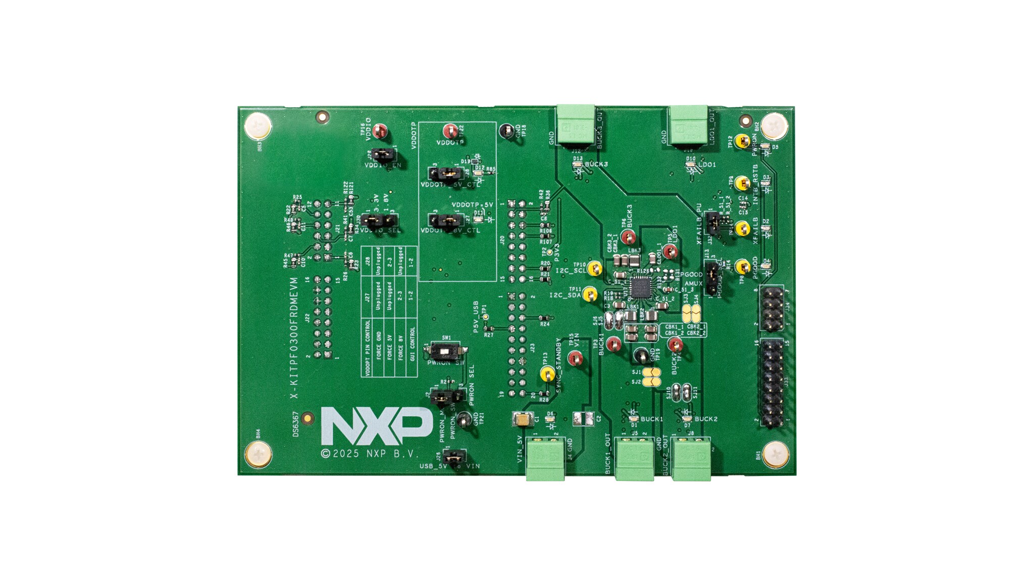
KITPF0300FRDMEVMキットは、NXPのPF0300 PMICをベースとした設計を評価するための統合プラットフォームです。PF0300のすべての機能がテスト環境でアクセスおよび監視できます。
キットのハードウェアは、KITPF0300FRDMEVM評価ボード、FRDM-KL25Zマイクロコントローラ・ボード、およびFRDM-KL25ZをPCに接続するためのUSBケーブルで構成されています。
KITPF0300FRDMEVM評価ボードには、個別のPF0300がはんだ付けされています。ボード上のコネクタ、ジャンパ、スイッチを使用して、特定の設計要件を満たした評価環境を構成できます。このボードに搭載されたLEDとテスト・ポイントを使用して、リアルタイムでパフォーマンスを監視することもできます。
KITPF0300FRDMEVMボードの底面にあるArduinoコネクタには、FRDM-KL25Zが取り付けられています。FRDM-KL25Zの役割は、KITPF0300FRDMEVMボードとPCにインストールされたGUI間のシリアル・ペリフェラル・インターフェース (SPI) 通信を管理することです。FRDM-KL25Zには、PCに接続されたUSBケーブルから電力が供給されます。
2.1 ボードの特長
- スイッチおよびLDO用Phoenix (3.81 mm) オス・コネクタ
- デバッグ・モード、通常モード、テスト・モードを選択可能
- 異なるモードでデバイスを起動するVDDOTPおよびPWRON
- PGOOD、INTB/RSTB、SYNC、およびXFAILピン
- ソフトウェアGUIへの接続を容易にするUSB to I²Cプロトコル
- 信号またはレギュレータの状態を示す緑色と赤色のLED
- VDDOTPピンの設定が8 V(OTP書き込み電圧)であることを示す青色LED
- 出力を監視するためのヘッダ・コネクタ
- KL25 MCU ADCによる高度なシステム監視
2.2 ボードのコンポーネント
| 位置 | 機能 | 説明 |
|---|---|---|
J4 |
VIN | 入力電圧(最小3.3 V/最大5.5 V) |
J5 |
BUCK1_OUT | Buck 1の出力 |
J8 |
BUCK2_OUT | Buck 2の出力 |
J12 |
BUCK3_OUT | Buck 3の出力 |
J16 |
LDO1_OUT | LDO 1の出力 |
J2 |
PWRON_SEL | PWRONをMCUで制御、またはPWRON_SWで手動制御 |
SW1 |
PWRON_SW | PWRONの手動制御(PWRON_SW位置のJ2を想定) |
J26 |
USB_5V_TO_VIN | USBから5 VをVINに供給(電流は1 Aに制限) |
J30 |
VDDIO_SEL | VDDIOを1.8 Vまたは3.3 Vに設定 |
J29 |
VDDIO_EN | VDDIOをVDDIOピンに印加 |
J13 |
PGOOD_SEL | PGOOD設定をPGOOD/GPOまたは接合部温度アナログ電圧出力に設定 |
J27 |
VDDOTP_8V_CTL | 手動またはMCUで制御されたVDDOTPの8 V |
J28 |
VDDOTP_5V_CTL | 手動またはMCUで制御されたVDDOTPの5 V |
J32 |
XFAILB_PU | XFAILBをVDDIOにプルアップ |
J33/J34 |
ヘッダを監視 | 監視用のI/Oピンとレギュレータ出力 |
SJ5 |
— | BUCK1_OUTとBUCK1_FBを接続するためのはんだジャンパ |
SJ6 |
— | BUCK1_LXとBUCK3_OUTを接続するためのはんだジャンパ |
3. ハードウェアの構成
3.1 ハードウェアの構成
KITPF0300FRDMEVMボードの設定手順は次のとおりです。
- 図1に示すように、ボードのジャンパがデフォルト位置に設定されていることを確認します。このデフォルト構成では、FRDM-KL25ZおよびGUIによるボードの完全な制御が可能になります
-
電源を
J4(Phoenixコネクタ - 3.81 mm)に接続します。電源は、初期値である5.0 Vに設定する必要があります - FRDM-KL25ZボードがKITPF0300FRDMEVMボードにしっかりと取り付けられていることを確認します。また、FRDM-KL25ZとPC間のUSBケーブルが確実に接続されていることを確認してください。この接続は、極めて重要となります。USBポートはPCとFRDM-KL25Zボード間の通信チャネルとして機能するだけでなく、一部のオンボード回路に電圧とリファレンスを供給し、集積回路 (IC) のVDDIOリファレンスを生成するためです。