データ・シート (1)
-
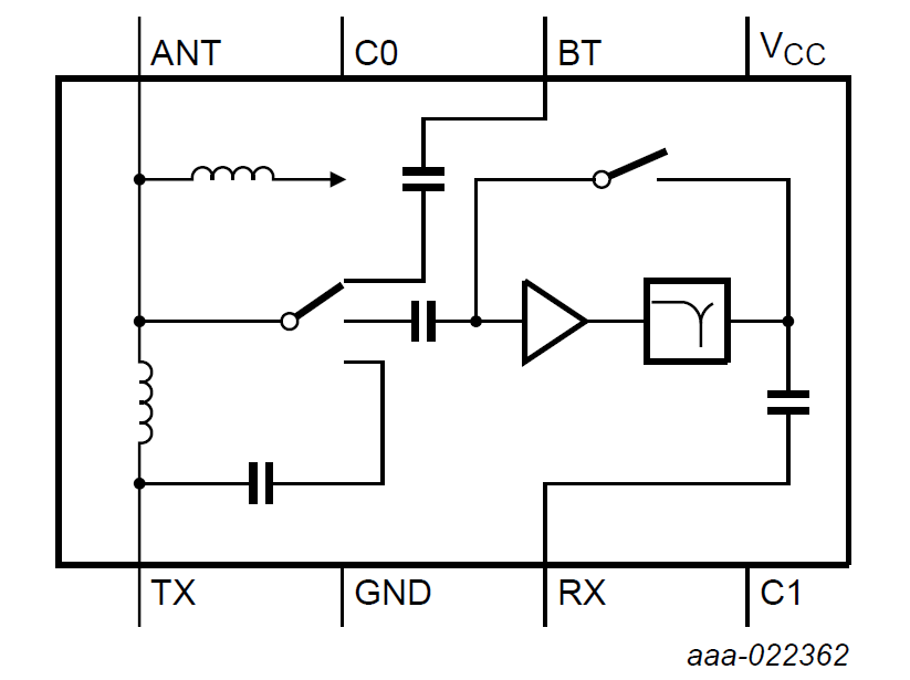
Archived - WLAN LNA+Switch[BGS8424]
The BGS8424 is, also known as the WLAN3101H, a fully integrated MMIC low-noise amplifier, and SP3T switch for Bluetooth® path and transmit path. For WLAN applications in the 2.4 GHz to 2.5 GHz ISM band. Manufactured using the high performance QUBiC eighth generation SiGe:C technology of NXP®.
The BGS8424 couples good noise figure, linearity, efficiency, low insertion loss. Also the CMOS switches with the process stability and ruggedness are the hallmarks of the SiGe:C technology.
The BGS8424 has a 1.5 mm × 1.5 mm footprint HX2SON8 package and a maximum thickness of 330 μm.
|
|
|
|
|
|
|
|---|---|---|---|---|---|
|
|
|
|
|
|
|
|
|
|
|
|
|
|
|
|
|
|
|
|
|
|
|
|
|
|
|
|
|
|
|
|
|
|
|
|
|
|
|
|
|
|
|
|
|
|
|
|
|
|
|
|
|
|
|
|
|
|
|
|
|
|
|
|
|
|
|
|
|
|
完全な内訳を受け取ります。 製品の設置面積などについては、 eCad ファイル.
