長期製品供給
対象製品には最低10年間の製品供給サポートが適用されます。自動車、通信、医療の各セグメント向けに開発された指定対象製品については、最低15年間の製品供給が保証されます。
NX5P3090は、USB PDアプリケーション向けに設計された、調整可能な高精度の電流制限電源スイッチです。このデバイスには、低電圧ロックアウト、過熱保護、および逆電流保護回路が搭載され、フォルト状態の発生時にはスイッチ端子を自動的に絶縁します。29VトレラントなVBUSピンにより、デバイスはUSB PDポートで動作できます。電流制限入力 (ILIM) ピンで過電流制限しきい値を定義し、オープン・ドレインのフォルト出力 (FAULT) が障害状態の発生を示します。
ILIMピンとGNDピンの間に外付け抵抗を使用して、過電流制限しきい値を400 mA~3.3 Aの範囲でプログラムできます。過電流状態では、デバイスは出力電流をILIMによる設定値にクランプし、FAULTフラグのアサート中はスイッチをオンに保持します。オン/オフ時の電流サージを最小限に抑えるために、電源スイッチの立上がり/立下がり時間を制御するソフト・スタートを内蔵しています。
システムの堅牢性を高めるため、デバイスにはサージ保護が組み込まれています。イネーブル入力にはロジック・レベル変換が内蔵され、デバイスは低電圧のプロセッサやコントローラと互換性があります。
NX5P3090は、12バンプ、1.35 x 1.65 mm、0.4 mmピッチのWLCSPパッケージで供給されます。
対象製品には最低10年間の製品供給サポートが適用されます。自動車、通信、医療の各セグメント向けに開発された指定対象製品については、最低15年間の製品供給が保証されます。
|
|
|
|
|
|
|
|---|---|---|---|---|---|
|
|
|
|
|
|
|
|
|
|
|
|
|
|
|
|
|
|
|
|
|
|
|
|
|
|
|
|
|
|
|
|
|
|
|
|
|
|
|
|
|
|
|
|
|
|
|
|
|
|
|
|
|
|
|
|
|
|
|
|
|
|
|
|
|
|
|
|
|
|
完全な内訳を受け取ります。 製品の設置面積などについては、 eCad ファイル.
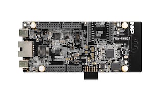
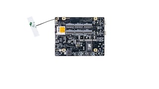
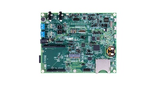
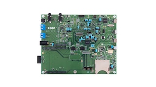
1-5 件/全 6 ハードウェア提供
NXPから直接サポートを受けるには、以下のサイトをご覧ください。 エンジニアリング・サービス.
1 エンジニアリング・サービス

この製品をサポートするその他のパートナー製品を見つけるには、当社の Web サイトにアクセスしてください パートナーマーケットプレイス.