- アナログ・ツールボックス
- DEMO-BYL1-EVB評価ボードのスタート・ガイド
DEMO-BYL1-EVB評価ボードのスタート・ガイド
このドキュメントの内容
-
パッケージの内容
-
ハードウェアの入手
-
ハードウェアの構成
サインイン 進行状況を保存するには アカウントをお持ちでない方 アカウントを作成する。
お客様の DEMO-BYL1-EVB
1. パッケージの内容
NXPのアナログ製品開発ボードは、NXP製品の評価を目的とした使いやすいプラットフォームです。さまざまなアナログ・ソリューション、ミックスド・シグナル・ソリューション、パワー・ソリューションに対応しています。実績のある大容量テクノロジを使用したモノリシック集積回路およびシステム・イン・パッケージ (SiP) デバイスを搭載しています。NXP製品は、最先端システムへの電源供給において、より長いバッテリー寿命、より小さいフォーム・ファクタ、より少ない部品数、より低いコスト、より優れたパフォーマンスを実現します。
このページでは、DEMO-BYL1-EVB評価ボードをセットアップして使用する手順について説明します。
1.1 キットの内容と同梱物一覧
DEMO-BYL1-EVBの内容物は次のとおりです。
- 組立て済み/テスト済みの評価ボード(静電気防止バッグ入り)
- 3.0フィートのUSB-STD A to USB-B-miniケーブル
- ボードに搭載されたジャンパ
- クイック・スタート・ガイド
1.2 追加ハードウェア
このキットの作業をする際は、キットの内容物のほかに以下のハードウェアが必要になるか、または使用すると役立ちます。
- 12 V電源、電流制限2.0 A(初期値)
1.3 ソフトウェア
BYLinkマルチプロセッサ・デモ・ボードを使用する前に、PCワークステーションに次のソフトウェアをインストールしておく必要があります。
- BYLink NXP GUIインストール・パッケージ
2. ハードウェアの入手
2.1 ボードの特長
- 電源入力用コネクタ
- PMICレギュレータ用のコネクタおよびテスト・ポイント
- OTPエミュレーションとPWRON
- ソフトウェアGUIへの接続を容易にするUSB to I²Cプロトコル
- 信号またはレギュレータの状態を示す緑色と赤色のLED
2.2 ボードの説明
BYLinkマルチプロセッサ・デモ・ボード・キットは、NXPのFS8500およびPF502x PMICデバイス・ファミリを搭載した設計を評価するための統合プラットフォームです。テスト環境ですべてのPMIC機能にアクセスし、監視できます。キットに含まれるハードウェアは、BYLinkマルチ・プロセッサ・デモ・ボードと、ボードをPCに接続するために必要なUSBケーブルです。
ボード上のコネクタ、ジャンパ、スイッチを使用して、特定の設計要件を満たした評価環境を構成できます。このボードに搭載されたLEDとテスト・ポイントを使用して、リアルタイムでパフォーマンスを監視することもできます。
2.3 キットの主なコンポーネント
DEMO-BYL1-EVBボードの概要
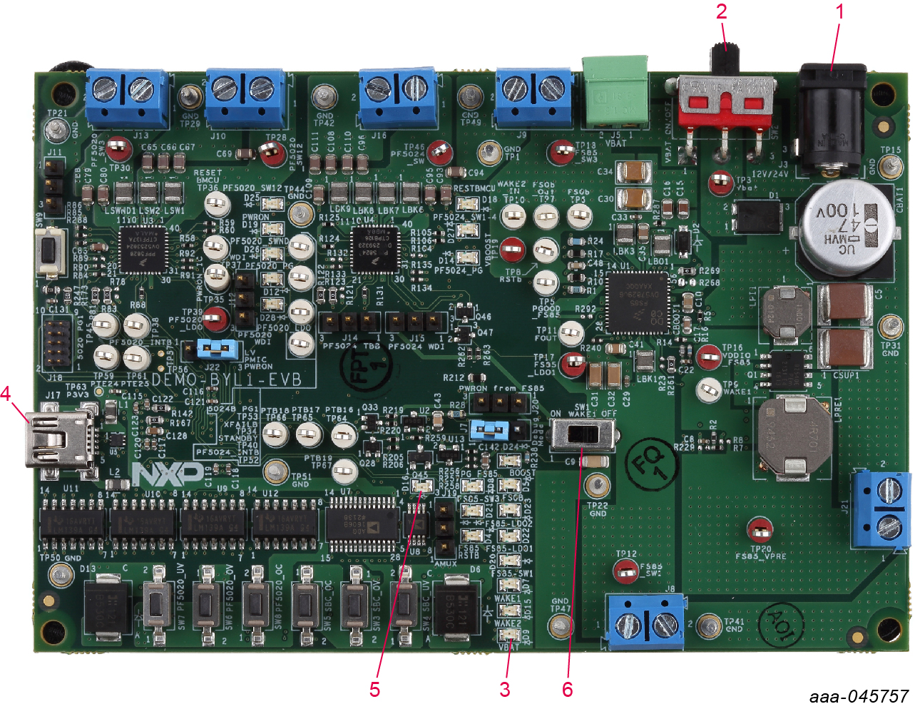
- 電源コネクタ
- 電源スイッチ
- VBAT LED
- USBコネクタ
- USB LED
SW1(WAKE1) スイッチ
3. ハードウェアの構成
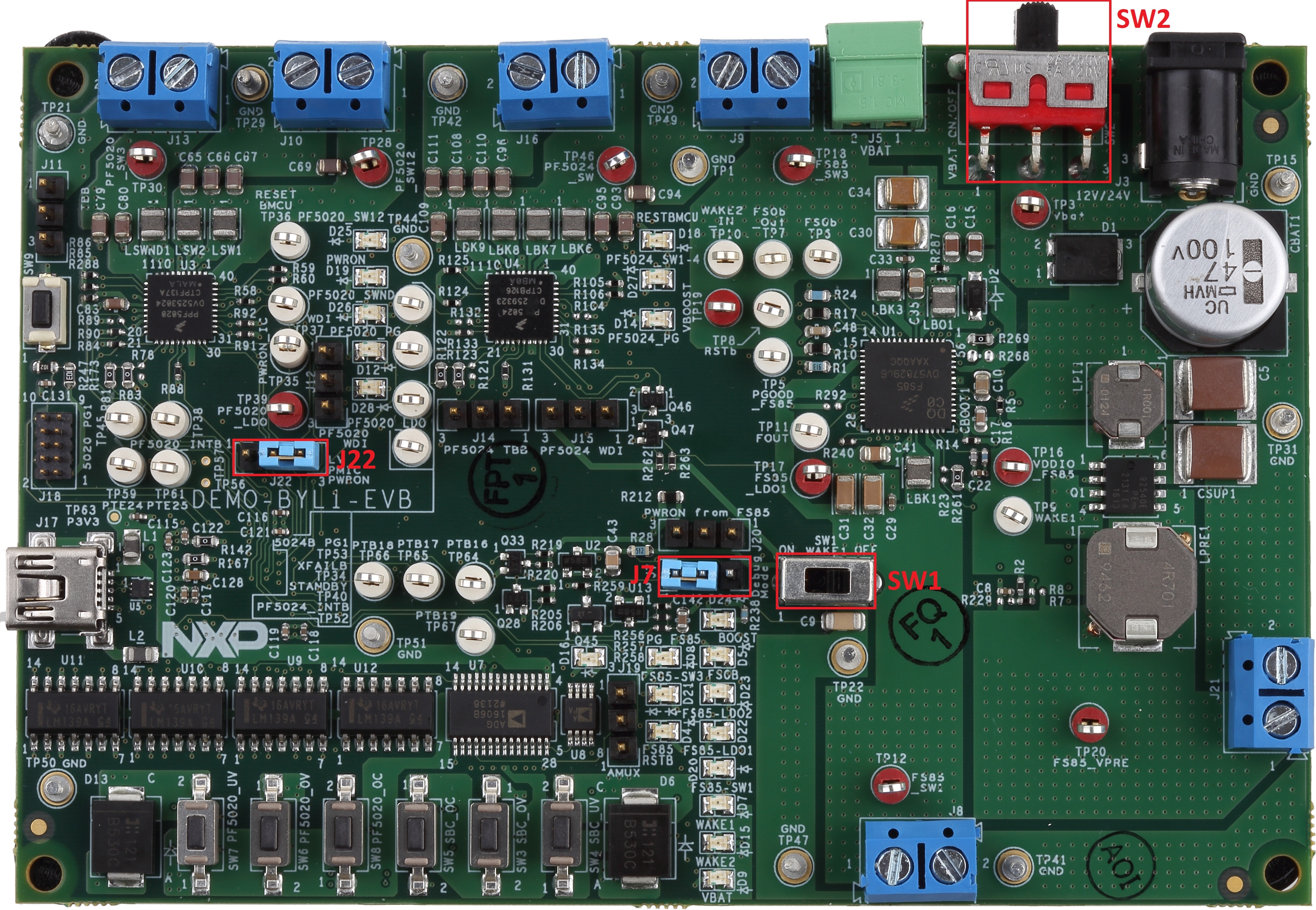
3.1 BYLinkマルチプロセッサの設定
BYLinkマルチプロセッサ・デモ・ボードの設定手順は次のとおりです。
- ボード上のジャンパが、次の図に示すようにデフォルト位置に設定されていることを確認します。このデフォルト設定の場合、MCUとGUIによってボードを完全に制御できます
- 電源を
J5(VBATおよびGND)に接続します。電源は12 Vの初期値に設定し、電流を2.0 Aに制限する必要があります - デモ・ボードとPCの間のUSBケーブルがしっかりと接続されていることを確認してください。この接続は極めて重要です。USBポートはPCとボード間の通信チャネルとして機能するだけでなく、一部のオンボード回路に電圧とリファレンスを供給するためです
SW1を中央位置から左位置1-2に切り替えて、VBATを12 V電源に接続します- 電源を
J3に接続する場合は、SW1を中央位置から右位置2-3に切り替えます
3.2 ハードウェアの構成
BYLinkマルチプロセッサ・デモ・ボードの設定手順は次のとおりです。
- ボード上のジャンパが、次の図に示すようにデフォルト位置に設定されていることを確認します。このデフォルト設定の場合、MCUとGUIによってボードを完全に制御できます
- 電源を
J5(VBATおよびGND)に接続します。電源は12 Vの初期値に設定し、電流を2.0 Aに制限する必要があります - デモ・ボードとPCの間のUSBケーブルがしっかりと接続されていることを確認してください。この接続は極めて重要です。USBポートはPCとボード間の通信チャネルとして機能するだけでなく、一部のオンボード回路に電圧とリファレンスを供給するためです
SW1を中央位置から左位置1-2に切り替えて、VBATを12 V電源に接続します- 電源を
J3に接続する場合は、SW1を中央位置から右位置2-3に切り替えます
設計・リソース
その他の参考情報
DEMO-BYL1-EVB:BYLinkマルチプロセッサ・デモ・ボードに加えて、次のサイトもご覧ください。
アプリケーション・ページ:
- PF5020:車載アプリケーション向けマルチチャネル (5) PMIC:高電力 x 4および低消費電力 x 1、ASIL Bセーフティ・レベルに適合
- PF5024:車載アプリケーション向けマルチチャネル (4) PMIC:高電力 x 4、ASIL Bセーフティ・レベルに適合
- FS8400:S32マイクロコントローラ用セーフティ・システム・ベーシス・チップ、ASIL Bに適合
- FS8500:S32マイクロコントローラ用セーフティ・システム・ベーシス・チップ、ASIL Dに適合
- BYLinkシステム電源プラットフォーム
アプリケーション・ページ:
ハードウェア・ページ:
ソフトウェア・ページ: