アプリケーション・ノート (1)
カタログ (1)
-
パワー・マネジメント集積回路 (PMIC) – パンフレット[PMICBRA4]
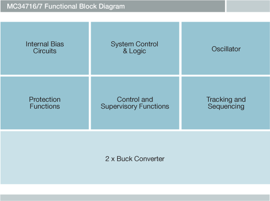
The NXP® MC34716 is a highly integrated, space-efficient, low cost, dual synchronous buck switching regulator with integrated N-channel power MOSFETs.
|
|
|
|
|
|
|
|---|---|---|---|---|---|
|
|
|
|
|
|
|
|
|
|
|
|
|
|
|
|
|
|
|
|
|
|
|
|
|
|
|
|
|
|
|
|
|
|
|
|
|
|
|
|
|
|
|
|
|
|
|
|
|
|
|
|
|
|
|
|
|
|
|
|
|
|
|
|
|
|
|
|
|
|
クイック・リファレンス ドキュメンテーションの種類
6 ドキュメント
コンパクトリスト
完全な内訳を受け取ります。 製品の設置面積などについては、 eCad ファイル.

