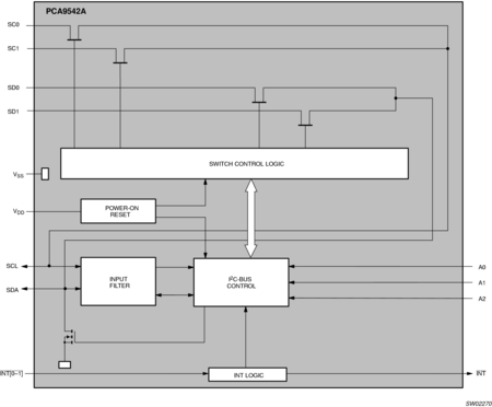
The PCA9542A is a 1-of-2 bidirectional translating multiplexer, controlled via the I²C-bus. The SCL/SDA upstream pair fans out to two SCx/SDx downstream pairs, or channels. Only one SCx/SDx channel is selected at a time, determined by the contents of the programmable control register. Two interrupt inputs, INT0 and INT1, one for each of the SCx/SDx downstream pairs, are provided. One interrupt output, INT, which acts as an AND of the two interrupt inputs, is provided.
A power-on reset function puts the registers in their default state and initializes the I²C-bus state machine with no channels selected.
The pass gates of the multiplexer are constructed such that the VDD pin can be used to limit the maximum high voltage which will be passed by the PCA9542A. This allows the use of different bus voltages on each SCx/SDx pair, so that 1.8 V, 2.5 V, or 3.3 V parts can communicate with 5 V parts without any additional protection. External pull-up resistors pull the bus up to the desired voltage level for each channel. All I/O pins are 5 V tolerant.